National Semiconductor LP38691 LP38693 User's Manual and Specifications
Summary
These low dropout CMOS linear regulators provide highly stable power management solutions with excellent precision and a wide operating temperature range. Ideal for applications requiring reliable power conversion, these components feature extremely low dropout voltage and are optimized for use with ceramic output capacitors. The accompanying documentation details the electrical specifications, pin descriptions (V, GND, OUT, EN), connection diagrams, and ordering information crucial for design engineers. They are perfect for portable instrumentation, notebook computers, battery-powered devices, and hard disk drives needing high reliability power supplies.
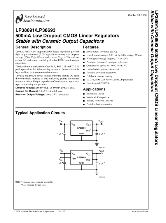
Page 1 Text Content
/L ro t C in r R la to rs ta le ith ra ic tp t C ito rs
October 24, 2008
LP38691/LP38693 500m A Low Dropout CMOS Linear Regulators Stable with Ceramic Output Capacitors General Description Features The LP38691/3 low dropout CMOS linear regulators provide 2.0% output accuracy (25°C) tight output tolerance (2.0% typical), extremely low dropout
Low dropout voltage: 250 m V @ 500m A (typ, 5V out)
voltage (250 m V @ 500m A load current, VOUT = 5V), and ex-
Wide input voltage range (2.7V to 10V)
cellent AC performance utilizing ultra low ESR ceramic output
Precision (trimmed) bandgap reference
capacitors.
Guaranteed specs for -40°C to +125°C
The low thermal resistance of the LLP, SOT-223 and T0-252
packages allow the full operating current to be used even in 1µA off-state quiescent current
high ambient temperature environments. Thermal overload protection The use of a PMOS power transistor means that no DC base Foldback current limiting drive current is required to bias it allowing ground pin current
T0-252, SOT-223 and 6-Lead LLP packages
to remain below 100 µA regardless of load current, input volt-
Enable pin (LP38693)
age, or operating temperature. Dropout Voltage: 250 m V (typ) @ 500m A (typ. 5V out).
Applications
Ground Pin Current: 55 µA (typ) at full load.
Hard Disk Drives
Precision Output Voltage: 2.0% (25°C) accuracy.
Notebook Computers Battery Powered Devices Portable Instrumentation
Typical Application Circuits
Note: * Minimum value required for stability. **LLP package devices only.
© 2008 National Semiconductor Corporation www.national.com
Page Summary Contents For National Semiconductor LP38691 LP38693 User's Manual and Specifications
Manual Details
| Brand | National |
|---|---|
| Pages | 16 |
| File Size | 363.63 KB |
| Published | June 17, 2026 |
Enter the captcha to get the download link:

Frequently Asked Questions
What is the typical low dropout voltage rating?
It provides a typical low dropout of 250 mV @ 500mA.
Are ceramic capacitors necessary for stable function?
Yes, the regulator requires ceramic output capacitors to achieve stability.
How can I eliminate error due to voltage drops in long traces?
Utilize the Sense pin (SNS) by connecting it and tying it directly to the OUT pin.
What is the guaranteed operating temperature range?
The device is rated for operation from -40°C up to +125°C.