# A B C D E F G H I J K L M N O P Q R S T U V W X Y Z

National Semiconductor - LM2524D LM3524D Regulating PWM Controller Data Sheet Manual

Summary

This comprehensive manual provides technical specifications for the LM2524D/LM3524D, a high-precision Pulse Width Modulator (PWM) regulating device. It is designed for engineers requiring reliable power regulation and a stable ±1% precision 5V reference in sensitive electronic systems. The document details operational capabilities across electrical sections—including output voltage, oscillator, and error-amplifier performance—covering absolute maximum ratings, temperature ranges, and crucial characteristics like noise suppression and synchronization features for demanding industrial and commercial designs.
📄 Preview 📖 Table of Contents Contents PAGE OF 22

Page 1 Text Content

/L la tin ls id th la to

May 2, 2008

LM2524D/LM3524D Regulating Pulse Width Modulator

pulse per period even in noisy environments. The LM3524D

General Description

includes double pulse suppression logic that insures when a

The LM3524D family is an improved version of the industry shut-down condition is removed the state of the T-flip-flop will standard LM3524. It has improved specifications and addi- change only after the first clock pulse has arrived. This feature tional features yet is pin for pin compatible with existing 3524 prevents the same output from being pulsed twice in a row, families. New features reduce the need for additional external thus reducing the possibility of core saturation in push-pull circuitry often required in the original version. designs. The LM3524D has a ±1% precision 5V reference. The current carrying capability of the output drive transistors has been Features raised to 200 m A while reducing VCEsat and increasing VCE

Fully interchangeable with standard LM3524 family

breakdown to 60V. The common mode voltage range of the

±1% precision 5V reference with thermal shut-down

error-amp has been raised to 5.5V to eliminate the need for

a resistive divider from the 5V reference. Output current to 200 m A DC In the LM3524D the circuit bias line has been isolated from 60V output capability

the shut-down pin. This prevents the oscillator pulse ampli-

Wide common mode input range for error-amp

tude and frequency from being disturbed by shut-down. Also

One pulse per period (noise suppression)

at high frequencies (≃300 k Hz) the max. duty cycle per output

Improved max. duty cycle at high frequencies

has been improved to 44% compared to 35% max. duty cycle

in other 3524s. Double pulse suppression In addition, the LM3524D can now be synchronized external- Synchronize through pin 3

ly, through pin 3. Also a latch has been added to insure one

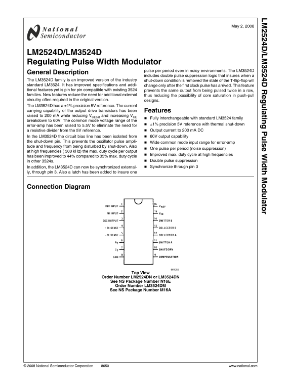
Connection Diagram

Top View

Order Number LM2524DN or LM3524DN See NS Package Number N16E Order Number LM3524DM See NS Package Number M16A

© 2008 National Semiconductor Corporation www.national.com

Page Summary Contents For National Semiconductor - LM2524D LM3524D Regulating PWM Controller Data Sheet Manual

Page 1 /L la tin ls id th la to May 2, 2008 LM2524D/LM3524D Regulating Pulse Width Modulator pulse per period even in noisy environments. The LM3524D General Description includes double pulse suppression log...
Page 2 Block Diagram www.national.com
Page 3 Internal Power Dissipation 1W Absolute Maximum Ratings (Note 5) Operating Junction Temperature If Military/Aerospace specified devices are required, Range (Note 2) please contact the National Semicond...
Page 4 LM2524D LM3524D Symbol Parameter Conditions Tested Design Tested Design Units Typ Limit Limit Typ Limit Limit (Note 3) (Note 4) (Note 3) (Note 4) Sawtooth Valley RT = 5.6k, CT = 0.01 μF 1.1 0.8 0.6 0....
Page 5 /L LM2524D LM3524D Symbol Parameter Conditions Tested Design Tested Design Units Typ Limit Limit Typ Limit Limit (Note 3) (Note 4) (Note 3) (Note 4) Common Mode −0.7 −0.7 VMin Voltage Range V5 − V4 = ...
Page 6 Typical Performance Characteristics Switching Transistor Maximum Average Power Peak Output Current Dissipation (N, M Packages) vs Temperature Maximum & Minimum Output Transistor Duty Cycle Thresho...
Page 7 /L Standby Current Standby Current vs Voltage vs Temperature Current Limit Sense Voltage Test Circuit www.national.com
Page 8 Functional Description INTERNAL VOLTAGE REGULATOR The LM3524D has an on-chip 5V, 50 m A, short circuit pro- tected voltage regulator. This voltage regulator provides a supply for all internal circuitr...
Page 9 The output of the amplifier, or input to the pulse width modu- /L CURRENT LIMITING lator, can be overridden easily as its output impedance is very The function of the current limit amplifier is to ove...
Page 10 Typical Applications FIGURE 7. Positive Regulator, Step-Up Basic Configuration (IIN(MAX) = 80 m A) FIGURE 8. Positive Regulator, Step-Up Boosted Current Configuration www.national.com
Page 11 FIGURE 9. Positive Regulator, Step-Down Basic Configuration (IIN(MAX) = 80 m A) www.national.com
Page 12 FIGURE 10. Positive Regulator, Step-Down Boosted Current Configuration FIGURE 11. Boosted Current Polarity Inverter www.national.com
Page 13 BASIC SWITCHING REGULATOR THEORY /L The circuit works as follows: Q1 is used as a switch, which AND APPLICATIONS has ON and OFF times controlled by the pulse width modu- The basic circuit of a step-do...
Page 14 Also, see LM1578 data sheet for graphical methods of induc- /L tor selection. CALCULATING OUTPUT FILTER CAPACITOR Co: Figure 13 shows L1's current with respect to Q1's t ON and t OFF times (VA is at t...
Page 15 *Mounted to Staver Heatsink No. V5-1. Q1 = BD344 Q2 = 2N5023 L1 = >40 turns No. 22 wire on Ferroxcube No. K300502 Torroid core. FIGURE 15. 5V, 1 Amp Step-Down Switching Regulator www.national.com
Page 16 TABLE 1. Parameter Conditions Typical Characteristics Output Voltage VIN = 10V, Io = 1A 5V Switching Frequency VIN = 10V, Io = 1A 20 k Hz Short Circuit VIN = 10V 1.3A Current Limit Load Regulation VIN...
Page 17 THE STEP-UP SWITCHING REGULATOR /L Figure 18 shows the basic circuit for a step-up switching reg- ulator. In this circuit Q1 is used as a switch to alternately apply VIN across inductor L1. During the...
Page 18 In calculating the output capacitor Co it can be seen that Co where: L1 is in henrys, f is the switching frequency in Hz /L supplies Io during t ON. The voltage change on Co during this To apply the a...
Page 19 L1 = > 25 turns No. 24 wire on Ferroxcube No. K300502 Toroid core. FIGURE 20. 15V, 0.5A Step-Up Switching Regulator FIGURE 21. Replacing R3/R4 Divider in Figure 20 with Reference Circuit Improves L...
Page 20 Physical Dimensions inches (millimeters) unless otherwise noted Molded Surface-Mount Package (M) Order Number LM3524DM NS Package Number M16A www.national.com
Page 21 Molded Dual-In-Line Package (N) Order Number LM2524DN or LM3524DN NS Package Number N16E www.national.com
Page 22 /L la ti ls id th la to Notes For more National Semiconductor product information and proven design tools, visit the following Web sites at: Products Design Support Amplifiers www.national.com/amplifi...

Manual Details

Brand National
Pages 22
File Size 1.05 MB
Published May 27, 2026
91 views

Enter the captcha to get the download link:

captcha

Frequently Asked Questions

What are the primary benefits of using the LM3524D over previous models?

It features double pulse suppression logic for noise resistance, an improved high-frequency duty cycle up to 44%, and a ±1% precision 5V reference.

Is the LM3524D compatible with standard parts families?

Yes, it is pin-for-pin compatible and fully interchangeable with existing standard LM2524 and LM3524 families.

What is the maximum continuous output current capability?

The output current (DC) for both models has been increased to 200 mA.

How can the device be externally synchronized?

It can be synchronized externally through pin 3, which also supports a dedicated latch connection.