National Semiconductor ADC08100 Data Sheet
Summary
This professional manual details the ADC081000, a high-performance 8-Bit Analog-to-Digital Converter (ADC) built for sophisticated signal acquisition. Capable of reaching 1 GSPS, this low-power CMOS device ensures robust conversion across industrial temperatures. It is designed for engineers working on demanding systems, including RADAR/SONAR, digital oscilloscopes, RF down converters, and advanced communications equipment that require guaranteed high resolution and minimal code errors.
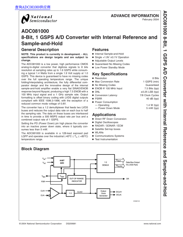
Page 1 Text Content
查询ADC081000供应商
ADVANCE INFORMATION
8-B it,1 /D onverter ith Internal R eference and am ple-and-H old
February
ADC081000 8-Bit, GSPS A/D Converter with Internal Reference and Sample-and-Hold General Description Features
NOTE: This product is currently in development. ALL Internal Sample-and-Hold
specifications are design targets and are subject to Single +1.9V ±0.1V Operation
change. Adjustable Output Levels
The ADC081000 is low power, high performance CMOS Guaranteed No Missing Codes
analog-to-digital converter that digitizes signals to bits Low Power Standby Mode resolution at sampling rates up to 1.6 GSPS while consum- ing typical 1.4 Watts from single 1.9 Volt supply at 1.0
Key Specifications
GSPS. This device is guaranteed to have no missing codes
Resolution Bits
over the full operating temperature range. The unique
Max Conversion Rate GSPS (min)
folding/interpolating architecture, the fully differential com-
parator design and the innovative design of the internal No Missing Codes Guaranteed sample-and-hold amplifier enable very flat SINAD/ENOB ENOB MHz Input 7.5 Bits (typ)
response beyond Nyquist, producing high 7.5 ENOB with DNL ±0.25 LSB (typ) MHz input signal and GHz sample rate. Output
Conversion Latency 7/8 Clock Cycles
formatting is offset binary coding with LVDS digital outputs
PSRR d B (typ)
compliant with IEEE 1596.3-1996, with the exception of
Power Consumption
reduced common mode voltage of 0.8V.
Operating 1.4 (typ)
The converter has 1:2 demultiplexer that feeds two LVDS
Power Down Mode m W (typ)
buses and reduces the output data rate on each bus to half the sampling rate. The data on these buses are interleaved
Applications
in time to provide MSPS output rate per bus and
Direct RF Down Conversion
combined output rate of GSPS.
Digital Oscilloscopes
Setting the PD (Power Down) pin high places the converter
RADAR SONAR ECM
into an inactive power down state, where it typically con-
sumes less than m W. Satellite Set-top boxes WLANs
The ADC081000 is available in 128-lead exposed pad
LQFP and operates over the industrial (-40o C TA +85o C) Communications Systems temperature range. Test Instrumentation
Block Diagram
National Semiconductor Corporation DS200681 www.national.com
Page Summary Contents For National Semiconductor ADC08100 Data Sheet
Manual Details
| Brand | National |
|---|---|
| Pages | 3 |
| File Size | 109.51 KB |
| Published | June 06, 2026 |
Enter the captcha to get the download link:

Frequently Asked Questions
What is the maximum operating temperature range?
The device operates over an industrial temperature range of -40 °C to +85 °C.
How much does the converter consume during normal operation?
Typical power consumption is 1.4 Watts from a single 1.9 Volt supply.
What are the main features of this 8-bit A/D Converter?
It features an internal Sample-and-Hold amplifier, guaranteed no missing codes, and has fully differential comparator design.
Under what conditions can I put it into a low power state?
Setting the PD (Power Down) pin high puts the converter into an inactive power down state, consuming typically less than 5 mW.