National Semiconductor MM74HC164 Data Sheet
Summary
This comprehensive manual provides technical details for the MM74HC164, a high-speed 8-bit serial-in/parallel-out shift register IC. Ideal for engineers integrating precise digital data shifting into complex circuit designs. The guide covers electrical specifications, absolute maximum ratings, functional pinouts, and availability across various packages (SOIC, TSSOP, PDIP), ensuring reliable integration into your electronic projects.
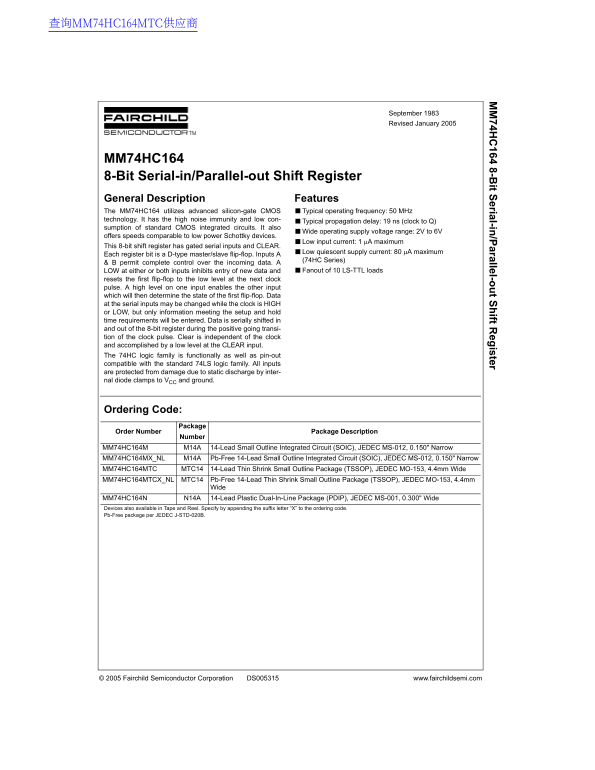
Page 1 Text Content
查询MM74HC164MTC供应商
74H 164 8-B it S erial-in /P arallel-o t S ift R eg ister
September 1983 Revised January 2005
MM74HC164 8-Bit Serial-in/Parallel-out Shift Register General Description Features The MM74HC164 utilizes advanced silicon-gate CMOS ■Typical operating frequency: 50 MHz technology. It has the high noise immunity and low con-
■Typical propagation delay: 19 ns (clock to Q)
sumption of standard CMOS integrated circuits. It also
■Wide operating supply voltage range: 2V to 6V
offers speeds comparable to low power Schottky devices.
■Low input current: 1 µA maximum
This 8-bit shift register has gated serial inputs and CLEAR.
■Low quiescent supply current: 80 µA maximum
Each register bit is a D-type master/slave flip-flop. Inputs A
(74HC Series)
& B permit complete control over the incoming data. A
LOW at either or both inputs inhibits entry of new data and ■Fanout of 10 LS-TTL loads
resets the first flip-flop to the low level at the next clock pulse. A high level on one input enables the other input which will then determine the state of the first flip-flop. Data at the serial inputs may be changed while the clock is HIGH or LOW, but only information meeting the setup and hold time requirements will be entered. Data is serially shifted in and out of the 8-bit register during the positive going transi- tion of the clock pulse. Clear is independent of the clock and accomplished by a low level at the CLEAR input. The 74HC logic family is functionally as well as pin-out compatible with the standard 74LS logic family. All inputs are protected from damage due to static discharge by inter- nal diode clamps to VCC and ground.
Ordering Code:
Package
Order Number Package Description
Number
MM74HC164M M14A 14-Lead Small Outline Integrated Circuit (SOIC), JEDEC MS-012, 0.150" Narrow MM74HC164MX_NL M14A Pb-Free 14-Lead Small Outline Integrated Circuit (SOIC), JEDEC MS-012, 0.150" Narrow MM74HC164MTC MTC14 14-Lead Thin Shrink Small Outline Package (TSSOP), JEDEC MO-153, 4.4mm Wide MM74HC164MTCX_NL MTC14 Pb-Free 14-Lead Thin Shrink Small Outline Package (TSSOP), JEDEC MO-153, 4.4mm
MM74HC164N N14A 14-Lead Plastic Dual-In-Line Package (PDIP), JEDEC MS-001, 0.300" Wide Devices also available in Tape and Reel. Specify by appending the suffix letter “X” to the ordering code. Pb-Free package per JEDEC J-STD-020B.
© 2005 Fairchild Semiconductor Corporation DS005315 www.fairchildsemi.com
Page Summary Contents For National Semiconductor MM74HC164 Data Sheet
Manual Details
| Brand | National |
|---|---|
| Pages | 7 |
| File Size | 73.59 KB |
| Published | June 04, 2026 |
Enter the captcha to get the download link:

Frequently Asked Questions
How can I reset the shift register without using the clock?
Use the dedicated CLEAR input; clearing is independent of the clock and requires a low level.
What logic family is this chip compatible with?
The 74HC logic family is functionally as well as pin-out compatible with the standard 74LS logic family.
How does data enter and exit the register?
Data is serially shifted in and out of the 8-bit register during the positive going transition of the clock pulse.
What are the electrical limitations for using this device?
The device has a wide operating supply voltage range, supporting operation between 2V to 6V.