National Semiconductor DS90CF384A DS90CF364A Data Sheet
Summary
These high-speed LVDS Receiver ICs are essential components designed for modern Flat Panel Display (FPD) interfaces. They reliably convert complex, wide high-speed data streams into standardized parallel CMOS/TTL signals. This device is ideal for electrical engineers and display system designers seeking a solution to eliminate EMI issues associated with traditional TTL connections. The manual provides comprehensive details on electrical characteristics, operational parameters (including power consumption and junction limits), ensuring accurate integration across various VGA, SVGA, and XGA configurations while maintaining signal integrity up to 65 MHz.
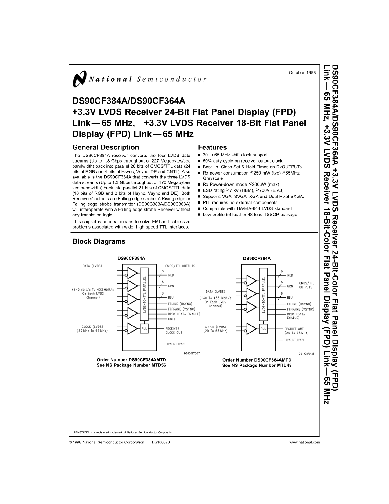
Page 1 Text Content
90C F384A /D 90C F364A +3.3V LV eceiver 24-B it-C olor Flat anel D isplay (FP Link z,+3.3V LV eceiver 18-B it-C olor Flat anel D isplay (FP Link
October
DS90CF384A/DS90CF364A +3.3V LVDS Receiver 24-Bit Flat Panel Display (FPD) Link—65 MHz, +3.3V LVDS Receiver 18-Bit Flat Panel Display (FPD) Link—65 MHz General Description Features
The DS90CF384A receiver converts the four LVDS data to MHz shift clock support
streams (Up to 1.8 Gbps throughput or Megabytes/sec 50% duty cycle on receiver output clock bandwidth) into parallel bits of CMOS/TTL data (24 Best–in–Class Set Hold Times on Rx OUTPUTs bits of RGB and bits of Hsync, Vsync, DE and CNTL). Also Rx power consumption <250 m W (typ) @65MHz available is the DS90CF364A that converts the three LVDS Grayscale data streams (Up to 1.3 Gbps throughput or Megabytes/
Rx Power-down mode <200µW (max)
sec bandwidth) into parallel bits of CMOS/TTL data
ESD rating >7 k V (HBM), >700V (EIAJ)
(18 bits of RGB and bits of Hsync, Vsync and DE). Both
Supports VGA, SVGA, XGA and Dual Pixel SXGA.
Receivers’ outputs are Falling edge strobe. Rising edge or
PLL requires no external components
Falling edge strobe transmitter (DS90C383A/DS90C363A)
will interoperate with Falling edge strobe Receiver without Compatible with TIA/EIA-644 LVDS standard any translation logic. Low profile 56-lead or 48-lead TSSOP package
This chipset is an ideal means to solve EMI and cable size problems associated with wide, high speed TTL interfaces.
Block Diagrams
DS90CF384A DS90CF364A
DS100870-27 DS100870-28
Order Number DS90CF384AMTD Order Number DS90CF364AMTD See NS Package Number MTD56 See NS Package Number MTD48
TRI-STATE® is registered trademark of National Semiconductor Corporation.
National Semiconductor Corporation DS100870 www.national.com
Page Summary Contents For National Semiconductor DS90CF384A DS90CF364A Data Sheet
Manual Details
| Brand | National |
|---|---|
| Pages | 14 |
| File Size | 307.53 KB |
| Published | July 22, 2026 |
Enter the captcha to get the download link:

Frequently Asked Questions
Which display standard resolutions does this receiver support?
It supports VGA, SVGA, XGA, and Dual Pixel SXGA signal types.
Is special componentry needed for the timing signals?
No external components are required for a PLL, as the outputs use a falling edge strobe.
How power-efficient is this device in standby mode?
The power-down mode offers very low consumption, retaining a maximum of <200μW.
What compatibility standards does it adhere to?
It is compatible with the TIA/EIA-644 LVDS standard and interoperates with falling edge strobe transmitters.