National Semiconductor DM5474 DM7474 Data Sheet
Summary
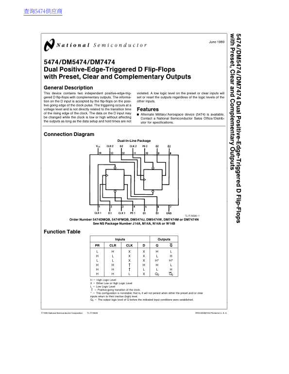
A reliable dual D Flip-Flop integrated circuit designed for capturing, storing, and synchronizing data within digital logic systems. This robust component features positive-edge triggering, along with built-in preset/clear functionality and complementary outputs for advanced interfacing. The accompanying technical documentation provides comprehensive electrical characteristics, precise timing specifications (setup/hold times), and operating limits necessary for engineers integrating high-performance memory components into their circuits.
Page 1 Text Content
itiv -E -T rig re lip -F lo
ith re t, le le ta ry tp ts 5474/DM5474/DM7474 Dual Positive-Edge-Triggered Flip-Flops with Preset, Clear and Complementary Outputs General Description
This device contains two independent positive-edge-trig- violated. low logic level on the preset or clear inputs will gered flip-flops with complementary outputs. The informa- set or reset the outputs regardless of the logic levels of the tion on the input is accepted by the flip-flops on the posi- other inputs.
tive going edge of the clock pulse. The triggering occurs at voltage level and is not directly related to the transition time Features of the rising edge of the clock. The data on the input may
Alternate Military/Aerospace device (5474) is available.
be changed while the clock is low or high without affecting
Contact National Semiconductor Sales Office/Distrib-
the outputs as long as the data setup and hold times are not
utor for specifications.
Connection Diagram
Dual-In-Line Package
TL/F/6526–1
Order Number 5474DMQB, 5474FMQB, DM5474J, DM5474W, DM7474M or DM7474N
See NS Package Number J14A, M14A, N14A or W14B
Function Table
Inputs Outputs
PR CLR CLK
High Logic Level Either Low or High Logic Level Low Logic Level Positive-going transition of the clock. This configuration is nonstable; that is, it will not persist when either the preset and/or clear inputs return to their inactive (high) level. Q0 The output logic level of before the indicated input conditions were established.
C1995 National Semiconductor Corporation TL/F/6526 RRD-B30M105/Printed in U. S. A.
Page Summary Contents For National Semiconductor DM5474 DM7474 Data Sheet
Manual Details
| Brand | National |
|---|---|
| Pages | 6 |
| File Size | 122.40 KB |
| Published | May 29, 2026 |
Enter the captcha to get the download link:

Frequently Asked Questions
What are the main functions of this D Flip-Flop?
It has independent preset, clear inputs, and provides complementary outputs for reliable data handling.
Are different parts suitable for varying temperatures?
Yes. The DM54 models support 55°C to 125°C, while the DM74 models are rated for 0°C to 70°C.
How strict are the timing requirements when connecting this chip?
The input setup time (SU) must be at least 20ns, and the input hold time (H) must be at least 5ns.
Can I use these components in critical medical equipment like life support systems?
No. Usage requires the express written approval of the National Semiconductor Corporation President.