National Semiconductor CLC5665 Data Sheet
Summary
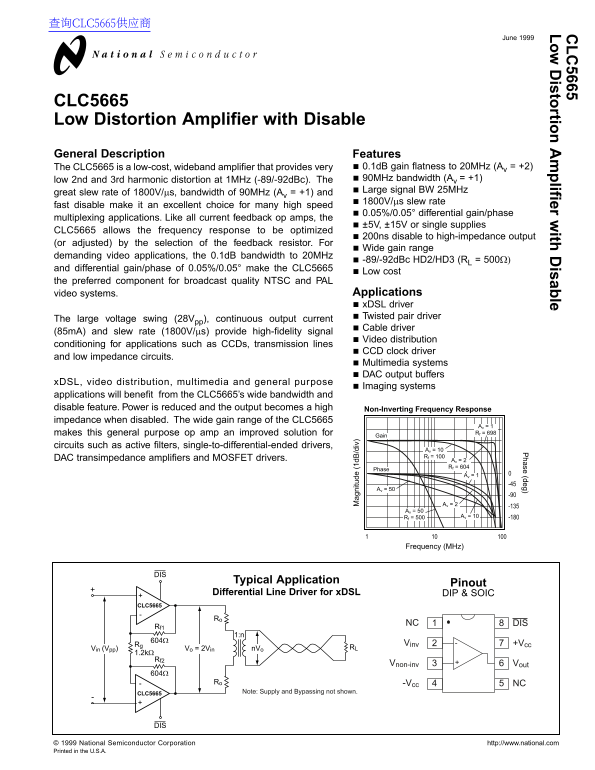
The CLC5665 is a high-speed, low-distortion wideband amplifier designed for rigorous signal processing demands. Featuring up to 90MHz bandwidth, an efficient disable mode, and excellent slew rates, it ensures superior performance in critical video distribution, DSL/twisted pair driving, and multimedia applications. The included technical manual provides comprehensive details on operational parameters, guaranteeing optimal circuit design for developers building high-fidelity systems ranging from broadcast quality NTSC/PAL to general demanding electronics.
Page 1 Text Content
查询CLC5665供应商
June 1999
isto rtio lifier w ith isab le
hase (deg)
CLC5665 Low Distortion Amplifier with Disable General Description Features
The CLC5665 is a low-cost, wideband amplifier that provides very 0.1d B gain flatness to 20MHz (Av = +2) low 2nd and 3rd harmonic distortion at 1MHz (-89/-92d Bc). The 90MHz bandwidth (Av = +1) Large signal BW 25MHz
great slew rate of 1800V/µs, bandwidth of 90MHz (Av = +1) and
1800V/µs slew rate
fast disable make it an excellent choice for many high speed
0.05%/0.05° differential gain/phase
multiplexing applications. Like all current feedback op amps, the
±5V, ±15V or single supplies
CLC5665 allows the frequency response to be optimized
200ns disable to high-impedance output
(or adjusted) by the selection of the feedback resistor. For
Wide gain range
demanding video applications, the 0.1d B bandwidth to 20MHz
-89/-92d Bc HD2/HD3 (RL = 500Ω)
and differential gain/phase of 0.05%/0.05° make the CLC5665
Low cost
the preferred component for broadcast quality NTSC and PAL
video systems. Applications x DSL driver Twisted pair driver
The large voltage swing (28Vpp), continuous output current
Cable driver
(85m A) and slew rate (1800V/µs) provide high-fidelity signal
Video distribution
conditioning for applications such as CCDs, transmission lines
CCD clock driver
and low impedance circuits. ag ni tu de 1d /d iv
Multimedia systems DAC output buffers
x DSL, video distribution, multimedia and general purpose
Imaging systems
applications will benefit from the CLC5665’s wide bandwidth and disable feature. Power is reduced and the output becomes a high Non-Inverting Frequency Response impedance when disabled. The wide gain range of the CLC5665
Av = 1 makes this general purpose op amp an improved solution for Rf = 698
circuits such as active filters, single-to-differential-ended drivers,
Av = 10 Rf = 100
DAC transimpedance amplifiers and MOSFET drivers. Av = 2
Rf = 604
Phase
Av = 1
Av = 50
Av = 2
Av = 50
Rf = 500 Av = 10 -180
Frequency (MHz)
Typical Application
Pinout
Differential Line Driver for x DSL DIP & SOIC
CLC5665
NC DIS
604ΩRg
inv +V cc
Vin (Vpp) Vo = 2Vin n Vo RL
1.2kΩ Rf2
non-inv out
Ro -V NC
CLC5665 Note: Supply and Bypassing not shown.
1999 National Semiconductor Corporation http://www.national.com Printed in the U.S.A.
Page Summary Contents For National Semiconductor CLC5665 Data Sheet
Manual Details
| Brand | National |
|---|---|
| Pages | 8 |
| File Size | 121.92 KB |
| Published | June 16, 2026 |
Enter the captcha to get the download link:

Frequently Asked Questions
What is the primary function of the enable/disable feature?
When disabled, the output current drops significantly, and the amplifier's output becomes high-impedance.
What bandwidth and slew rate should I know about?
It offers a 90MHz bandwidth (at A=+1) and boasts a fast slew rate of 1800 V/ms.
Can this component be used in life support systems?
No, use in life support or critical devices requires specific written approval from the manufacturer.