National Semiconductor 5442A DM5442A DM7442A Data Sheet
Summary
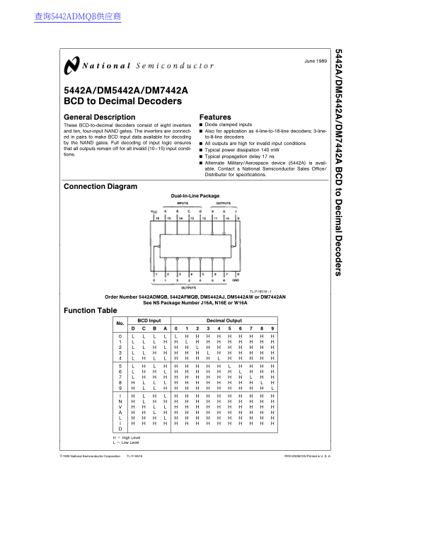
This BCD-to-Decimal Decoder integrated circuit is designed to reliably convert Binary Coded Decimal inputs into clear 0-9 logic outputs. This resource provides comprehensive technical documentation for engineers, including detailed function tables, electrical characteristics (voltages, timing), absolute maximum ratings, and operating guidelines necessary for system design. It serves as a crucial component in digital circuits requiring efficient signal decoding across various environmental conditions.
Page 1 Text Content
查询5442ADMQB供应商
to im rs
5442A/DM5442A/DM7442A BCD to Decimal Decoders General Description Features
These BCD-to-decimal decoders consist of eight inverters Diode clamped inputs
and ten, four-input NAND gates. The inverters are connect- Also for application as 4-line-to-16-line decoders; 3-line- ed in pairs to make BCD input data available for decoding to-8-line decoders by the NAND gates. Full decoding of input logic ensures All outputs are high for invalid input conditions that all outputs remain off for all invalid (10–15) input condi- Typical power dissipation m W tions.
Typical propagation delay ns Alternate Military/Aerospace device (5442A) is avail- able. Contact National Semiconductor Sales Office/ Distributor for specifications.
Connection Diagram
Dual-In-Line Package
TL/F/6516–1
Order Number 5442ADMQB, 5442AFMQB, DM5442AJ, DM5442AW or DM7442AN
See NS Package Number J16A, N16E or W16A
Function Table
BCD Input Decimal Output
High Level Low Level
C1995 National Semiconductor Corporation TL/F/6516 RRD-B30M105/Printed in U. S. A.
Page Summary Contents For National Semiconductor 5442A DM5442A DM7442A Data Sheet
Manual Details
| Brand | National |
|---|---|
| Pages | 6 |
| File Size | 119.60 KB |
| Published | June 17, 2026 |
Enter the captcha to get the download link:

Frequently Asked Questions
What is the required operating voltage for this decoder?
The supply voltage range is typically from 4.5V (Min) to 5.5V (Max).
How does the device function as a BCD-to-Decimal Decoder?
It uses eight inverters and ten four-input NAND gates to decode a 4-bit BCD input into a single corresponding decimal output line.
What is the typical propagation delay time for this decoder?
The typical PHL (High to Low) delay is 25 ns from A, B, C, or D through two levels of logic.
Do different package types affect compatibility?
Different packages include J16A, N16E, and W16A for ceramic/molded variations.