National LMX2330A LMX2331A LMX2332A Data Manual
Summary
This PLLatinum Dual Frequency Synthesizer provides high-stability RF and Intermediate Frequency (IF) local oscillator signals for demanding wireless systems. Utilizing advanced digital phase-locked loop technology, this component family is designed for applications in cellular/cordless communications, WLANs, and cable TV tuners. The manual offers comprehensive technical specifics, including operational voltage ranges (2.7V to 5.5V), full pin descriptions, and integration guides for models like the LMX2330A through LMX2332A, making it essential for wireless system designers.
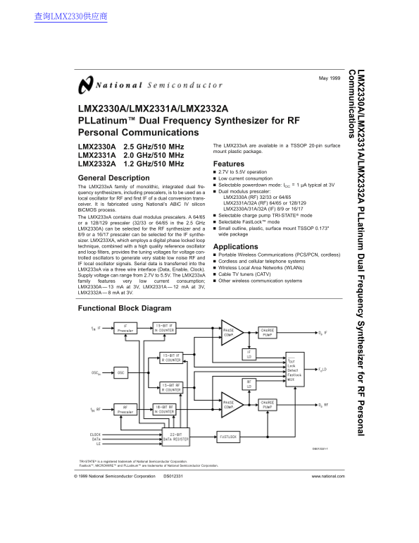
Page 1 Text Content
查询LMX2330供应商
LM 2330A /LM 2331A /LM 2332A LLatinum ual Frequency ynthesizer for ersonal om unications
LMX2330A/LMX2331A/LMX2332A PLLatinum™ Dual Frequency Synthesizer for RF Personal Communications
The LMX233x A are available in TSSOP 20-pin surface
LMX2330A 2.5 GHz/510 MHz
mount plastic package.
LMX2331A 2.0 GHz/510 MHz LMX2332A 1.2 GHz/510 MHz Features
2.7V to 5.5V operation General Description Low current consumption Selectable powerdown mode: ICC µA typical at 3V
The LMX233x A family of monolithic, integrated dual fre-
quency synthesizers, including prescalers, is to be used as Dual modulus prescaler: local oscillator for RF and first IF of dual conversion trans- LMX2330A (RF) 32/33 or 64/65 ceiver. It is fabricated using National’s ABi C IV silicon LMX2331A/32A (RF) 64/65 or 128/129 Bi CMOS process. LMX2330A/31A/32A (IF) 8/9 or 16/17 Selectable charge pump TRI-STATE® mode
The LMX233x A contains dual modulus prescalers. 64/65
or 128/129 prescaler (32/33 or 64/65 in the 2.5 GHz Selectable Fast Lock™ mode LMX2330A) can be selected for the RF synthesizer and Small outline, plastic, surface mount TSSOP 0.173" 8/9 or 16/17 prescaler can be selected for the IF synthe- wide package
sizer. LMX233XA, which employs digital phase locked loop technique, combined with high quality reference oscillator Applications and loop filters, provides the tuning voltages for voltage con-
Portable Wireless Communications (PCS/PCN, cordless)
trolled oscillators to generate very stable low noise RF and
Cordless and cellular telephone systems
IF local oscillator signals. Serial data is transferred into the
Wireless Local Area Networks (WLANs)
LMX233x A via three wire interface (Data, Enable, Clock).
Supply voltage can range from 2.7V to 5.5V. The LMX233x A Cable TV tuners (CATV) family features very low current consumption; Other wireless communication systems
LMX2330A m A at 3V, LMX2331A m A at 3V, LMX2332A m A at 3V.
Functional Block Diagram
DS012331-1
TRI-STATE® is registered trademark of National Semiconductor Corporation. Fastlock™, MICROWIRE™ and PLLatinum™ are trademarks of National Semiconductor Corporation.
National Semiconductor Corporation DS012331 www.national.com
Page Summary Contents For National LMX2330A LMX2331A LMX2332A Data Manual
Manual Details
| Brand | National |
|---|---|
| Pages | 17 |
| File Size | 395.72 KB |
| Published | June 04, 2026 |
Enter the captcha to get the download link:

Frequently Asked Questions
What is the operating voltage range for the LMX233xA family?
The supply voltage can range from 2.7V to 5.5V.
Which applications use the LMX233xA dual frequency synchronizer?
It is used in PCS/PCN, cordless phone systems, WLANs, CATV tuners, and other wireless communication systems.
What are the typical current draws for different models at 3V?
LMX2330A typically draws 13 mA, LMX2331A draws 12 mA, and LMX2332A draws 8 mA.
How is data transferred into the device's internal registers?
Serial data is provided via a three-wire interface (Data, Enable, Clock) with data inputting MSB first.