National DS40MB200 Data Manual
Summary
A specialized dual 2:1 multiplexer and 1:2 buffer designed for ultra-reliable, high-speed data paths up to 4 Gbps. This component enhances signal integrity in complex backplane systems using advanced features like controlled input equalization and programmable output pre-emphasis, compensating effectively for transmission losses on long FR4 substrates. The product manual provides detailed electrical specifications, pin descriptions, and functional diagrams required by engineers designing premium network infrastructure and demanding high-speed communication equipment.
Page 1 Text Content
查询DS40MB200供应商
August
40M ual4 b/s 1:2 ux/B uffer ith Input qualization and utput re-E phasis
DS40MB200 Dual Gb/s 1:2 Mux/Buffer with Input Equalization and Output Pre-Emphasis General Description Features
The DS40MB200 is dual signal conditioning 2:1 multi- Dual 2:1 multiplexer and 1:2 buffer plexer and 1:2 fan-out buffer designed for use in backplane 1– Gbps fully differential data paths
redundancy applications. Signal conditioning features in- Fixed input equalization clude input equalization and programmable output pre-
Programmable output pre-emphasis
emphasis that enable data communication in FR4 back-
Independent switch and line side pre-emphasis controls
planes up to Gb/s. Each input stage has fixed equalizer
Programmable switch-side loopback mode
to reduce ISI distortion from board traces. All output drivers
On-chip terminations
have selectable steps of pre-emphasis to compensate for
+3.3V supply
transmission losses from long FR4 backplanes and reduce
deterministic jitter. The pre-emphasis levels can be indepen- Low power, 1W max dently controlled for the line-side and switch-side drivers. Lead-less LLP-48 package (7mmx7mmx0.8mm, 0.5mm The internal loopback paths from switch-side input to switch- pitch)
side output enable at-speed system testing. All receiver 0˚C to +85˚C operating temperature range inputs and driver outputs are internally terminated with 100Ω differential terminating resistors
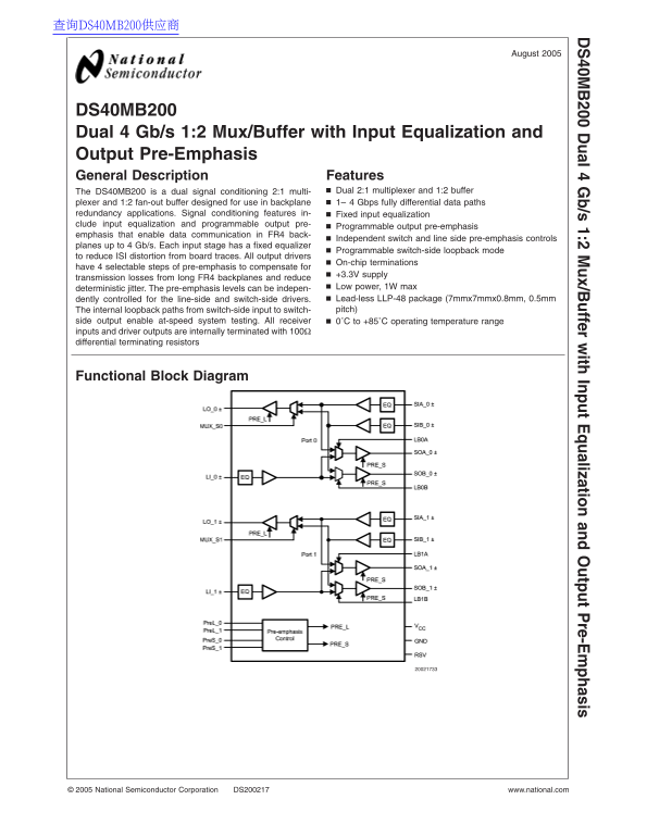
Functional Block Diagram
National Semiconductor Corporation DS200217 www.national.com
Page Summary Contents For National DS40MB200 Data Manual
Manual Details
| Brand | National |
|---|---|
| Pages | 14 |
| File Size | 1001.07 KB |
| Published | May 29, 2026 |
Enter the captcha to get the download link:

Frequently Asked Questions
What signal paths does the DS40MB200 support?
It is designed for 1–4 Gbps fully differential data paths, suitable for redundancy applications.
How can I control the output pre-emphasis settings?
Pre-emphasis levels are controlled by the PREL_x and PRES_x digital input pins.
Does the device support board testing or signal integrity verification?
Yes, it includes a programmable switch-side loopback mode to reduce ISI distortion from board traces.
What is the required operating temperature range for this module?
The inputs and driver outputs operate within an internal -20°C to +85°C temperature range.