# A B C D E F G H I J K L M N O P Q R S T U V W X Y Z

National LF155, LF156, LF256, LF257, LF355, LF356, LF357 JFET Input Operational Amplifiers Data Manual

Summary

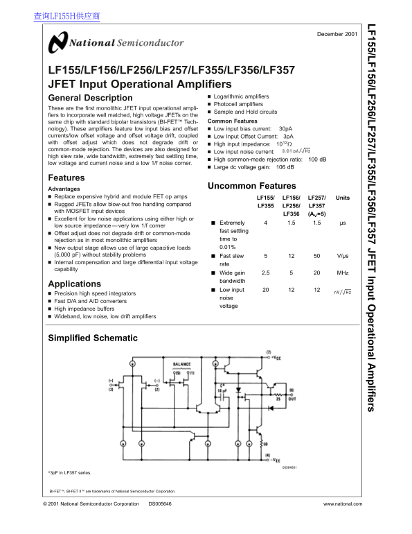
These advanced JFET input operational amplifiers are designed for high-precision and low-noise instrumentation systems. The manual provides comprehensive technical data covering electrical characteristics, optimal operating conditions, and key advantages such as ultralow input bias current, high common-mode rejection, and fast bandwidth. They are ideal for electronics engineers requiring robust performance in specialized circuits, including integrators, sample-and-hold units, or wideband signal conditioning applications.
📄 Preview PAGE OF 23

Page 1 Text Content

查询LF155H供应商

December

LF155/LF156/LF256/LF257/LF355/LF356/LF357 JFE Input perational A plifiers

LF155/LF156/LF256/LF257/LF355/LF356/LF357 JFET Input Operational Amplifiers

Logarithmic amplifiers

General Description

Photocell amplifiers

These are the first monolithic JFET input operational ampli-

Sample and Hold circuits

fiers to incorporate well matched, high voltage JFETs on the

same chip with standard bipolar transistors (BI-FET™ Tech- Common Features

nology). These amplifiers feature low input bias and offset Low input bias current: 30p A currents/low offset voltage and offset voltage drift, coupled Low Input Offset Current: 3p A with offset adjust which does not degrade drift or

High input impedance: 1012Ω

common-mode rejection. The devices are also designed for

Low input noise current:

high slew rate, wide bandwidth, extremely fast settling time,

High common-mode rejection ratio: d B

low voltage and current noise and low 1/f noise corner.

Large dc voltage gain: d B

Features

Uncommon Features

Advantages Replace expensive hybrid and module FET op amps LF155/ LF156/ LF257/ Units Rugged JFETs allow blow-out free handling compared

LF355 LF256/ LF357

with MOSFET input devices

LF356 (AV=5)

Excellent for low noise applications using either high or

Extremely 1.5 1.5 µs

low source impedance very low 1/f corner

fast settling

Offset adjust does not degrade drift or common-mode

rejection as in most monolithic amplifiers time to New output stage allows use of large capacitive loads 0.01%

(5,000 p F) without stability problems Fast slew V/µs Internal compensation and large differential input voltage

capability

Wide gain 2.5 MHz bandwidth

Applications

Low input

Precision high speed integrators

noise

Fast D/A and A/D converters

voltage

High impedance buffers Wideband, low noise, low drift amplifiers

Simplified Schematic

*3p F in LF357 series.

BI-FET™, BI-FET II™ are trademarks of National Semiconductor Corporation.

National Semiconductor Corporation DS005646 www.national.com

Page Summary Contents For National LF155, LF156, LF256, LF257, LF355, LF356, LF357 JFET Input Operational Amplifiers Data Manual

Page 1 查询LF155H供应商 December LF155/LF156/LF256/LF257/LF355/LF356/LF357 JFE Input perational A plifiers LF155/LF156/LF256/LF257/LF355/LF356/LF357 JFET Input Operational Amplifiers Logarithmic amplifiers Genera...
Page 2 Absolute Maximum Ratings (Note 1) If Military/Aerospace specified devices are required, contact the National Semiconductor Sales Office/Distributors LF for 5/ LF 6/ LF 6/ LF 7/ LF 5/ LF 6/ LF availabi...
Page 3 DC Electrical Characteristics (Continued) LF155/LF156/LF256/LF257/LF355/LF356/LF357 (Note 3) LF256/7 LF155/6 LF355/6/7 Symbol Parameter Conditions LF356B Units Min Typ Max Min Typ Max Min Typ Max IB I...
Page 4 Notes for Electrical Characteristics (Continued) LF 5/ LF 6/ LF 6/ LF 7/ LF 5/ LF 6/ LF LF155/156 LF256/257 LF356B LF355/6/7 Supply Voltage, VS ±15V VS ±20V ±15V VS ±20V ±15V VS ±20V VS= ±15V TA −55˚C...
Page 5 Typical DC Performance Characteristics Curves are for LF155 and LF156 unless otherwise LF155/LF156/LF256/LF257/LF355/LF356/LF357 specified. (Continued) Supply Current Supply Current Negative Current L...
Page 6 Typical DC Performance Characteristics Curves are for LF155 and LF156 unless otherwise specified. (Continued) LF 5/ LF 6/ LF 6/ LF 7/ LF 5/ LF 6/ LF Open Loop Voltage Gain Output Voltage Swing Typical...
Page 7 Typical AC Performance Characteristics (Continued) LF155/LF156/LF256/LF257/LF355/LF356/LF357 Output Impedance LF155 Small Signal Pulse Response, AV +1 LF156 Small Signal Pulse Response, AV +1 LF155 La...
Page 8 Typical AC Performance Characteristics (Continued) LF 5/ LF 6/ LF 6/ LF 7/ LF 5/ LF 6/ LF Inverter Settling Time Open Loop Frequency Response Bode Plot Bode Plot Bode Plot Common-Mode Rejection Ratio ...
Page 9 Typical AC Performance Characteristics (Continued) LF155/LF156/LF256/LF257/LF355/LF356/LF357 Power Supply Rejection Ratio Power Supply Rejection Ratio Undistorted Output Voltage Swing Equivalent Input...
Page 10 Detailed Schematic LF 5/ LF 6/ LF 6/ LF 7/ LF 5/ LF 6/ LF *C 3p F in LF357 series. Connection Diagrams (Top Views) Metal Can Package (H) Dual-In-Line Package (M and N) Order Number LF155H, LF156H, LF2...
Page 11 Application Hints (Continued) Typical Circuit Connections LF155/LF156/LF256/LF257/LF355/LF356/LF357 reversal of phase to the output. Exceeding the negative VOS Adjustment common-mode limit on both inp...
Page 12 Typical Applications LF 5/ LF 6/ LF 6/ LF 7/ LF 5/ LF 6/ LF Settling Time Test Circuit Settling time is tested with the LF155/6 connected as unity gain inverter and LF357 connected for AV −5 FET used ...
Page 13 Typical Applications (Continued) LF155/LF156/LF256/LF257/LF355/LF356/LF357 Low Drift Adjustable Voltage Reference VOUT/∆T ±0.002%/˚C All resistors and potentiometers should be wire-wound P1: drift adj...
Page 14 Typical Applications (Continued) LF 5/ LF 6/ LF 6/ LF 7/ LF 5/ LF 6/ LF Precision Current Monitor VO R1/R2 (V/m A of IS) R1, R2, R3: 0.1% resistors Use LF155 for Common-mode range to supply range Low ...
Page 15 Typical Applications (Continued) LF155/LF156/LF256/LF257/LF355/LF356/LF357 Wide BW Low Noise, Low Drift Amplifier Parasitic input capacitance C1 (3p F for LF155, LF156 and LF357 plus any additional la...
Page 16 Typical Applications (Continued) LF 5/ LF 6/ LF 6/ LF 7/ LF 5/ LF 6/ LF Decades VCO R1, R4 matched. Linearity 0.1% over decades. Isolating Large Capacitive Loads Overshoot 6% ts 10µs When driving larg...
Page 17 Typical Applications (Continued) LF155/LF156/LF256/LF257/LF355/LF356/LF357 Low Drift Peak Detector By adding D1 and Rf, VD1=0 during hold mode. Leakage of D2 provided by feedback path through Rf. Leak...
Page 18 Typical Applications (Continued) LF 5/ LF 6/ LF 6/ LF 7/ LF 5/ LF 6/ LF High Impedance, Low Drift Instrumentation Amplifier System VOS adjusted via A2 VOS adjust Trim R3 to boost up CMRR to d B. Instr...
Page 19 Typical Applications (Continued) LF155/LF156/LF256/LF257/LF355/LF356/LF357 Fast Sample and Hold Both amplifiers (A1, A2) have feedback loops individually closed with stable responses (overshoot neglig...
Page 20 Typical Applications (Continued) LF 5/ LF 6/ LF 6/ LF 7/ LF 5/ LF 6/ LF High Accuracy Sample and Hold By closing the loop through A2, the VOUT accuracy will be determined uniquely by A1. No VOS adjust...
Page 21 Typical Applications (Continued) LF155/LF156/LF256/LF257/LF355/LF356/LF357 High Notch Filter 2R1 10MΩ 2C C1 300p F Capacitors should be matched to obtain high f NOTCH Hz, notch −55 d B, Use LF155 for ...
Page 22 Physical Dimensions inches (millimeters) unless otherwise noted LF 5/ LF 6/ LF 6/ LF 7/ LF 5/ LF 6/ LF Metal Can Package (H) Order Number LF155H, LF156H, LF256H, LF257H, LF356BH, LF356H or LF357H NS P...
Page 23 Physical Dimensions inches (millimeters) unless otherwise noted (Continued) LF155/LF156/LF256/LF257/LF355/LF356/LF357 JFE Input perational A plifiers Molded Dual-In-Line Package (N) Order Number LF356...

Manual Details

Brand National
Pages 23
File Size 1.04 MB
Published June 01, 2026
84 views

Enter the captcha to get the download link:

captcha

Frequently Asked Questions

What is the main advantage of using BI-FET Technology in these amplifiers?

It integrates well matched high voltage JFETs and standard bipolar transistors onto a single chip, providing low input bias currents.

What is the typical Common-Mode Rejection Ratio (CMRR)?

The specified CMRR is typically 100 dB for most listed devices.

Are these chips suitable for critical life support medical equipment?

No. They are not authorized for use as critical components in life support systems without expressed written approval from National Semiconductor Corporation.