Page 1
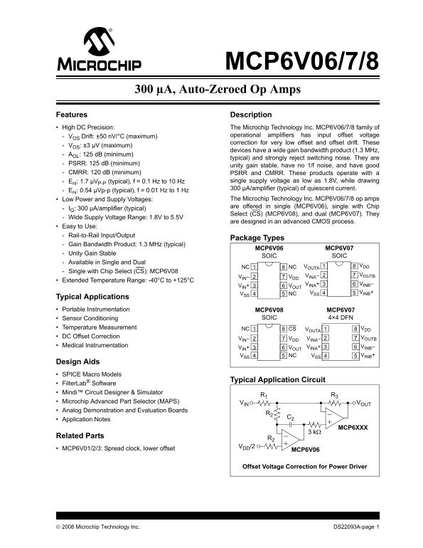
MCP6V06/7/8 µA, Auto-Zeroed Op Amps Features Description High DC Precision: The Microchip Technology Inc. MCP6V06/7/8 family of VOS Drift: ±50 n V/°C (maximum) operational amplifiers has input offset ...
Page 2
MCP6V06/7/8 1.0 ELECTRICAL CHARACTERISTICS 1.1 Absolute Maximum Ratings VDD VSS .......................................................................6.5V Notice: Stresses above those listed under “A...
Page 3
MCP6V06/7/8 TABLE 1-1: DC ELECTRICAL SPECIFICATIONS (CONTINUED) Electrical Characteristics: Unless otherwise indicated, TA = +25°C, VDD = +1.8V to +5.5V, VSS = GND, VCM = VDD/3, VOUT VDD/2, VL VDD/2, ...
Page 4
MCP6V06/7/8 TABLE 1-3: DIGITAL ELECTRICAL SPECIFICATIONS Electrical Characteristics: Unless otherwise indicated, TA = +25°C, VDD = +1.8V to +5.5V, VSS = GND, VCM = VDD/3, VOUT VDD/2, VL VDD/2, RL = 20...
Page 5
MCP6V06/7/8 1.3 Timing Diagrams 1.4 Test Circuits The circuits used for the DC and AC tests are shown in Figure 1-5 and Figure 1-6. Lay the bypass capacitors 1.8V to 5.5V1.8V VDD 0V out as discussed i...
Page 6
MCP6V06/7/8 2.0 TYPICAL PERFORMANCE CURVES Pe rc en ta ge f O cc ur re nc es Pe rc en ta ge f O cc ur re nc es Pe rc en ta ge f O cc ur re nc es Note: The graphs and tables provided following this not...
Page 7
MCP6V06/7/8 Note: Unless otherwise indicated, TA +25°C, VDD +1.8V to 5.5V, VSS GND, VCM VDD/3, VOUT VDD/2, VL VDD/2, RL kΩ to VL, CL = 60 p F, and CS GND. Pe rc en ta ge f O cc ur re nc es In pu t O f...
Page 8
MCP6V06/7/8 Note: Unless otherwise indicated, TA +25°C, VDD +1.8V to 5.5V, VSS GND, VCM In pu t B ia VDD/3, VOUT s, ffs et ur re nt VDD/2, In pu t B ia s, ffs et ur re nt pe n- Lo op ai (d VL VDD/2, R...
Page 9
MCP6V06/7/8 Note: Unless otherwise indicated, TA +25°C, VDD +1.8V to 5.5V, VSS GND, VCM VDD/3, VOUT VDD/2, VL VDD/2, RL kΩ to VL, CL = 60 p F, and CS GND. ut pu t H ea dr oo (m V) ut pu t V ol ta ge e...
Page 10
MCP6V06/7/8 Note: Unless otherwise indicated, TA +25°C, VDD +1.8V to 5.5V, VSS GND, VCM VDD/3, VOUT VDD/2, ri Vo lta ge (V VL VDD/2, RL kΩ to VL, CL = 60 p F, and CS GND. Ambient Temperature (°C) FIGU...
Page 11
MCP6V06/7/8 Note: Unless otherwise indicated, TA +25°C, VDD +1.8V to 5.5V, VSS GND, VCM VDD/3, VOUT VDD/2, VL VDD/2, RL kΩ to VL, CL = 60 p F, and CS GND. pe n- Lo op ai (d pe n- Lo op ai (d , P SR (d...
Page 12
MCP6V06/7/8 Note: Unless otherwise indicated, TA +25°C, VDD +1.8V to 5.5V, VSS GND, VCM pe n- Lo op VDD/3, VOUT ut pu t I pe da nc VDD/2, pe n- Lo op ut pu t I pe da nc VL VDD/2, RL kΩ to VL, CL = 60 ...
Page 13
MCP6V06/7/8 Note: Unless otherwise indicated, TA +25°C, VDD +1.8V to 5.5V, VSS GND, VCM VDD/3, VOUT VDD/2, VL VDD/2, RL kΩ to VL, CL = 60 p F, and CS GND. In pu t N oi se ol ta ge en si ty pu t N oi s...
Page 14
MCP6V06/7/8 Note: Unless otherwise indicated, TA +25°C, VDD +1.8V to 5.5V, VSS GND, VCM VDD/3, VOUT VDD/2, In pu t, ut pu t V ol ta ge (V In pu t O ffs et ol ta ge In pu t O ffs et ol ta ge (µ V) VL V...
Page 15
MCP6V06/7/8 Note: Unless otherwise indicated, TA +25°C, VDD +1.8V to 5.5V, VSS GND, VCM VDD/3, VOUT VDD/2, VL VDD/2, RL kΩ to VL, CL = 60 p F, and CS GND. Sl ew at (V /µ s) ut pu t V ol ta ge (V VDD =...
Page 16
MCP6V06/7/8 Note: Unless otherwise indicated, TA +25°C, VDD +1.8V to 5.5V, VSS GND, VCM VDD/3, VOUT VDD/2, Po er up pl ur re nt (µ Po er up pl ur re nt (µ hi Se le ct ur re nt (µ VL VDD/2, RL kΩ to VL...
Page 17
MCP6V06/7/8 Note: Unless otherwise indicated, TA +25°C, VDD +1.8V to 5.5V, VSS GND, VCM VDD/3, VOUT VDD/2, VL VDD/2, RL kΩ to VL, CL = 60 p F, and CS GND. hi Se le ct ur Ti hi Se le ct ys te re si (V ...
Page 18
MCP6V06/7/8 3.0 PIN DESCRIPTIONS Descriptions of the pins are listed in Table 3-1. TABLE 3-1: PIN FUNCTION TABLE MCP6V06 MCP6V07 MCP6V08 Symbol Description SOIC DFN, SOIC SOIC VOUT, VOUTA Output (op a...
Page 19
MCP6V06/7/8 4.0 APPLICATIONS 4.1 Overview of Auto-zeroing Operation The MCP6V06/7/8 family of auto-zeroed op amps is manufactured using Microchip’s state of the art CMOS Figure 4-1 shows a simplified ...
Page 20
MCP6V06/7/8 4.1.2 AUTO-ZEROING ACTION offset voltage on overall performance. Essentially, the Null Amplifier and Main Amplifier behave as a regular Figure 4-2 shows the connections between amplifiers ...
Page 21
MCP6V06/7/8 4.2 Other Functional Blocks pins (VIN+ and VIN–) from going too far above VDD, and dump any currents onto VDD. When implemented as 4.2.1 RAIL-TO-RAIL INPUTS shown, resistors R1 and R2 also...
Page 22
MCP6V06/7/8 4.3 Application Tips 4.3.5 CAPACITIVE LOADS Driving large capacitive loads can cause stability 4.3.1 INPUT OFFSET VOLTAGE OVER problems for voltage feedback op amps. As the load TEMPERATUR...
Page 23
MCP6V06/7/8 4.3.6 REDUCING UNDESIRED NOISE 4.3.8 PCB DESIGN FOR DC PRECISION AND SIGNALS In order to achieve DC precision on the order of ±1 µV, Reduce undesired noise and signals with: many physical ...
Page 24
MCP6V06/7/8 4.3.8.2 Non-inverting and Inverting Amplifier 4.3.8.3 Difference Amplifier Layout for Layout for Thermo-junctions Thermo-junctions Figure 4-9 shows the recommended non-inverting and Figure...
Page 25
MCP6V06/7/8 4.3.8.4 Dual Non-inverting Amplifier Layout 4.3.8.5 Other PCB Thermal Design Tips for Thermo-junctions In cases where an individual resistor needs to have its The dual op amp amplifiers sh...
Page 26
MCP6V06/7/8 4.3.8.6 Crosstalk 4.4 Typical Applications DC crosstalk causes offsets that appear as a larger 4.4.1 WHEATSTONE BRIDGE input offset voltage. Common causes include: Many sensors are configu...
Page 27
MCP6V06/7/8 4.4.2 RTD SENSOR gain is is set so that V4/THJ is 10 m V/°C. V3 represents the output of a temperature sensor, which produces a The ratiometric circuit in Figure 4-15 conditions a three vo...
Page 28
MCP6V06/7/8 The MCP1541 produces a 4.10V output, assuming 4.4.5 PRECISION COMPARATOR VDD is at 5.0V. This voltage, tied to a resistor ladder of Use high gain before a comparator to improve the 4.100R ...
Page 29
MCP6V06/7/8 5.0 DESIGN AIDS 5.5 Analog Demonstration and Evaluation Boards Microchip provides the basic design aids needed for the MCP6V06/7/8 family of op amps. Microchip offers a broad spectrum of A...
Page 30
MCP6V06/7/8 6.0 PACKAGING INFORMATION 6.1 Package Marking Information 8-Lead DFN (4x4) (MCP6V07) Example XXXXXX 6V07 XXXXXX E/MD^^ 3e YYWW NNN 8-Lead SOIC (150 mil) Example: XXXXXXXX MCP6VO6E XXXXYYWW...
Page 31
MCP6V06/7/8 EXPOSED PAD © 2008 Microchip Technology Inc. DS22093A-page 31
Page 32
MCP6V06/7/8 DS22093A-page 32 © 2008 Microchip Technology Inc.
Page 33
MCP6V06/7/8 © 2008 Microchip Technology Inc. DS22093A-page 33
Page 34
MCP6V06/7/8 NOTES: DS22093A-page 34 © 2008 Microchip Technology Inc.
Page 35
MCP6V06/7/8 APPENDIX A: REVISION HISTORY Revision A (June 2008) Original Release of this Document. © 2008 Microchip Technology Inc. DS22093A-page 35
Page 36
MCP6V06/7/8 APPENDIX B: OFFSET RELATED We use production screens to ensure the quality of our outgoing products. These screens are set at wider lim- TEST SCREENS its to eliminate any fliers; see Table...
Page 37
MCP6V06/7/8 PRODUCT IDENTIFICATION SYSTEM To order or obtain information, e.g., on pricing or delivery, refer to the factory or the listed sales office. PART NO. –X /XX Examples: a) MCP6V06T-E/SN: Ext...
Page 38
MCP6V06/7/8 NOTES: DS22093A-page 38 © 2008 Microchip Technology Inc.
Page 39
Note the following details of the code protection feature on Microchip devices: Microchip products meet the specification contained in their particular Microchip Data Sheet. Microchip believes that it...
Page 40
WORLDWIDE SALES AND SERVICE AMERICAS ASIA/PACIFIC ASIA/PACIFIC EUROPE Corporate Office Asia Pacific Office India - Bangalore Austria - Wels 2355 West Chandler Blvd. Tel: 91-80-4182-8400 Suites 3707-14...