# A B C D E F G H I J K L M N O P Q R S T U V W X Y Z

NEC Photocoupler PS9552, PS9552L1, PS9552L2, PS9552L3 2.5A Output Current, High CMR IGBT Gate Drive Photocoupler 8-Pin Dip Photocoupler Data Manual/Specifications

Summary

These opto-isolators are specialized photocouplers designed for robust power electronics applications, including industrial inverters and IGBT/MOS FET gate driving circuits. Engineered specifically for high common mode transient immunity (CMR), they ensure reliable signal isolation even under harsh electrical conditions. The manual provides comprehensive technical details, including specifications on high peak output current (up to 2.5 A), fast switching speeds, long creepage distances, multiple package options (DIP and surface mount), and detailed application guidelines for industrial power systems.
📄 Preview 📖 Table of Contents Contents PAGE OF 22

Page 1 Text Content

DATA SHEET

PHOTOCOUPLER

PS9552,PS9552L1,PS9552L2,PS9552L3 2.5 A OUTPUT CURRENT, HIGH CMR IGBT GATE DRIVE PHOTOCOUPLER 8-PIN DIP PHOTOCOUPLER −NEPOC Series−

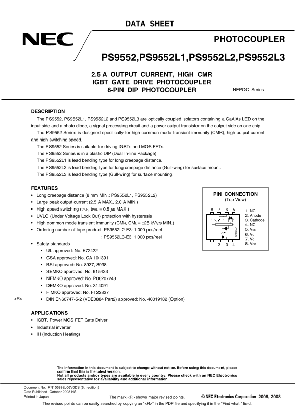
DESCRIPTION The PS9552, PS9552L1, PS9552L2 and PS9552L3 are optically coupled isolators containing a Ga Al As LED on the input side and a photo diode, a signal processing circuit and a power output transistor on the output side on one chip. The PS9552 Series is designed specifically for high common mode transient immunity (CMR), high output current and high switching speed. The PS9552 Series is suitable for driving IGBTs and MOS FETs. The PS9552 Series is in a plastic DIP (Dual In-line Package). The PS9552L1 is lead bending type for long creepage distance. The PS9552L2 is lead bending type for long creepage distance (Gull-wing) for surface mount. The PS9552L3 is lead bending type (Gull-wing) for surface mounting.

FEATURES

• Long creepage distance (8 mm MIN.: PS9552L1, PS9552L2) PIN CONNECTION (Top View)

• Large peak output current (2.5 A MAX., 2.0 A MIN.) • High speed switching (t PLH, t PHL = 0.5 μs MAX.)

1. NC • UVLO (Under Voltage Lock Out) protection with hysteresis 2. Anode 3. Cathode

• High common mode transient immunity (CMH, CML = ±25 k V/μs MIN.)

4. NC • Ordering number of tape product: PS9552L2-E3: 1 000 pcs/reel 5. VEE 6. VO

IE LD

: PS9552L3-E3: 1 000 pcs/reel

7. VO • Safety standards 8. VCC

• UL approved: No. E72422 • CSA approved: No. CA 101391 • BSI approved: No. 8937, 8938 • SEMKO approved: No. 615433 • NEMKO approved: No. P06207243 • DEMKO approved: No. 314091 • FIMKO approved: No. FI 22827 <R> • DIN EN60747-5-2 (VDE0884 Part2) approved: No. 40019182 (Option)

APPLICATIONS • IGBT, Power MOS FET Gate Driver • Industrial inverter • IH (Induction Heating)

The information in this document is subject to change without notice. Before using this document, please confirm that this is the latest version. Not all products and/or types are available in every country. Please check with an NEC Electronics sales representative for availability and additional information.

Document No. PN10589EJ06V0DS (6th edition) Date Published October 2008 NS Printed in Japan 2006, 2008 The mark <R> shows major revised points.

The revised points can be easily searched by copying an "<R>" in the PDF file and specifying it in the "Find what:" field.

Page Summary Contents For NEC Photocoupler PS9552, PS9552L1, PS9552L2, PS9552L3 2.5A Output Current, High CMR IGBT Gate Drive Photocoupler 8-Pin Dip Photocoupler Data Manual/Specifications

Page 1 DATA SHEET PHOTOCOUPLER PS9552,PS9552L1,PS9552L2,PS9552L3 2.5 A OUTPUT CURRENT, HIGH CMR IGBT GATE DRIVE PHOTOCOUPLER 8-PIN DIP PHOTOCOUPLER −NEPOC Series− DESCRIPTION The PS9552, PS9552L1, PS9552L2 a...
Page 2 PS9552,PS9552L1,PS9552L2,PS9552L3 PACKAGE DIMENSIONS (UNIT: mm) DIP Type PS9552 0 to 15˚ Lead Bending Type (Gull-wing) For Surface Mount PS9552L3 Data Sheet PN10589EJ06V0DS 2
Page 3 PS9552,PS9552L1,PS9552L2,PS9552L3 Lead Bending Type For Long Creepage Distance PS9552L1 2.54 0 to 15˚ Lead Bending Type (Gull-wing) For Long Creepage Distance (Surface Mount) PS9552L2 Data Sheet PN105...
Page 4 PS9552,PS9552L1,PS9552L2,PS9552L3 FUNCTIONAL DIAGRAM (Tr. 1) (Tr. 2) SHIELD Input LED Tr. 1 Tr. 2 Output ON ON OFF OFF OFF ON MARKING EXAMPLE No. 1 pin Mark Type Number NT831 Assembly Lot 31 N Week As...
Page 5 PS9552,PS9552L1,PS9552L2,PS9552L3 ORDERING INFORMATION Part Number Order Number Solder Plating Packing Style Safety Standard Application Part Specification Approval Number*1 PS9552 PS9552-AX Pb-Free M...
Page 6 PS9552,PS9552L1,PS9552L2,PS9552L3 ABSOLUTE MAXIMUM RATINGS (TA = 25°C, unless otherwise specified) Parameter Symbol Ratings Unit Diode Forward Current IF 25 m A Peak Transient Forward IF (TRAN) 1.0 A ...
Page 7 PS9552,PS9552L1,PS9552L2,PS9552L3 ELECTRICAL CHARACTERISTICS (TA = −40 to +100°C, VCC = 15 to 30 V, IF (ON) = 7 to 16 m A, VF (OFF) = −2 to 0.8 V, VEE = GND, unless otherwise specified) Parameter Symb...
Page 8 PS9552,PS9552L1,PS9552L2,PS9552L3 SWITCHING CHARACTERISTICS (TA = −40 to +100°C, VCC = 15 to 30 V, IF (ON) = 7 to 16 m A, VF (OFF) = −2 to 0.8 V, VEE = GND, unless otherwise specified) Parameter Symbo...
Page 9 PS9552,PS9552L1,PS9552L2,PS9552L3 TEST CIRCUIT Fig. 1 IOH Test Circuit Fig. 2 IOL Test Circuit 0.1 Fμ IOL VCC = 15 to 30 V IF = VCC = 7 to 16 m A IOH 15 to 30 V SHIELD SHIELD Fig. 3 VOH Test Circuit F...
Page 10 PS9552,PS9552L1,PS9552L2,PS9552L3 Fig. 7 t PLH, t PHL, tr, tf Test Circuit and Wave Forms 0.1 Fμ tr tf VCC = 15 to 30 VIF = 7 to 16 m A VO500 Ω 90% 10 k Hz 10 Ω 50% 50% DUTY CYCLE VOUT t PHLt PLH SHIE...
Page 11 PS9552,PS9552L1,PS9552L2,PS9552L3 hr es ho ld In pu t C ur re nt (m To ta l P ow er is si pa tio ax im um or ar ur re nt TYPICAL CHARACTERISTICS (TA = 25°C, unless otherwise specified) MAXIMUM FORWARD...
Page 12 PS9552,PS9552L1,PS9552L2,PS9552L3 ro pa ga tio el ay im t P L, t P LH ns ro pa ga tio el ay im t P L, t P LH ns ig Le ve l O ut pu t V ol ta ge up pl ul se id th is to rt io (P t P LH ns ul se id th i...
Page 13 PS9552,PS9552L1,PS9552L2,PS9552L3 ig Le ve l O ut pu t V ol ta ge up pl ig Le ve l S up pl ur re nt ig Le ve l O ut pu t C ur re nt ol ta ge Lo ev el up pl ur re nt (m SUPPLY CURRENT vs. SUPPLY CURREN...
Page 14 PS9552,PS9552L1,PS9552L2,PS9552L3 ro pa ga tio el ay im L, t P LH ns ul se id th is to rt io (P t P t P LH ns PROPAGATION DELAY TIME, PULSE WIDTH DISTORTION vs. LOAD RESISTANCE OUTPUT VOLTAGE vs. SUPP...
Page 15 PS9552,PS9552L1,PS9552L2,PS9552L3 TAPING SPECIFICATIONS (UNIT: mm) Outline and Dimensions (Tape) 4.0±0.1 +0.1 4.5 MAX. 1.5 –0 Tape Direction PS9552L2-E3 Outline and Dimensions (Reel) 23.9 to 27.4 Oute...
Page 16 PS9552,PS9552L1,PS9552L2,PS9552L3 Outline and Dimensions (Tape) 5.3 MAX. Tape Direction PS9552L3-E3 Outline and Dimensions (Reel) 15.9 to 19.4 Outer edge of Packing: 1 000 pcs/reel flange Data Sheet P...
Page 17 PS9552,PS9552L1,PS9552L2,PS9552L3 RECOMMENDED MOUNT PAD DIMENSIONS (UNIT: mm) Part Number Lead Bending lead bending type (Gull-wing) PS9552L2 10.2 2.54 1.7 2.2 for long creepage distance (surface moun...
Page 18 PS9552,PS9552L1,PS9552L2,PS9552L3 NOTES ON HANDLING 1. Recommended soldering conditions (1) Infrared reflow soldering ac ka ge ur fa ce em pe ra tu re ˚C • Peak reflow temperature 260°C or below (pack...
Page 19 PS9552,PS9552L1,PS9552L2,PS9552L3 (4) Cautions • Fluxes Avoid removing the residual flux with freon-based and chlorine-based cleaning solvent. 2. Cautions regarding noise Be aware that when voltage is...
Page 20 PS9552,PS9552L1,PS9552L2,PS9552L3 SPECIFICATION OF VDE MARKS LICENSE DOCUMENT Parameter Symbol Spec. Unit Application classification (DIN EN 60664-1 VDE0110 Part 1) for rated line voltages ≤ 300 Vr.m....
Page 21 PS9552,PS9552L1,PS9552L2,PS9552L3 The information in this document is current as of October, 2008. The information is subject to change without notice. For actual design-in, refer to the latest public...
Page 22 PS9552,PS9552L1,PS9552L2,PS9552L3 This product uses gallium arsenide (Ga As). Caution Ga As Products Ga As vapor and powder are hazardous to human health if inhaled or ingested, so please observe the ...

Manual Details

Brand Current
Pages 22
File Size 209.96 KB
Published May 28, 2026
82 views

Enter the captcha to get the download link:

captcha

Frequently Asked Questions

What key performance features define the PS9552 Series photocouplers?

The series is designed for high common mode transient immunity (CMR), a large peak output current (up to 2.5 A), and high switching speed (0.5 μs MAX.).

Which applications are recommended for using this type of photocoupler?

It is suitable for driving IGBTs and MOS FETs, particularly in industrial inverters and Induction Heating (IH) systems.

What differences exist between the various PS9552 package types?

PS9552L1 and PS9552L2 are lead bending types for long creepage distances, while PS9552L3 is specifically designed as a Gull-wing lead bending type for surface mounting.

What safety measures must be observed when disposing of this product?

It contains gallium arsenide (GaAs), so users must commission a licensed disposal company and never burn, cut, or crush the product.