MAXIM MAX4760 MAX4760A MAX4761 MAX4761A High-Bandwidth, Quad DPDT Switches
Summary
Maximize signal integrity in your portable devices with these high-bandwidth, low-capacitance analog switches. Engineered for reliable data and audio routing, the MAX476x series handles USB 1.1/2.0 signals while operating across a wide +1.8V to +5.5V range. This manual provides critical technical specifications, including electrical characteristics, pin configurations, and deep details on quad DPDT switches for applications in PDAs, notebooks, and cellular communication systems requiring robust high-speed signal switching solutions.
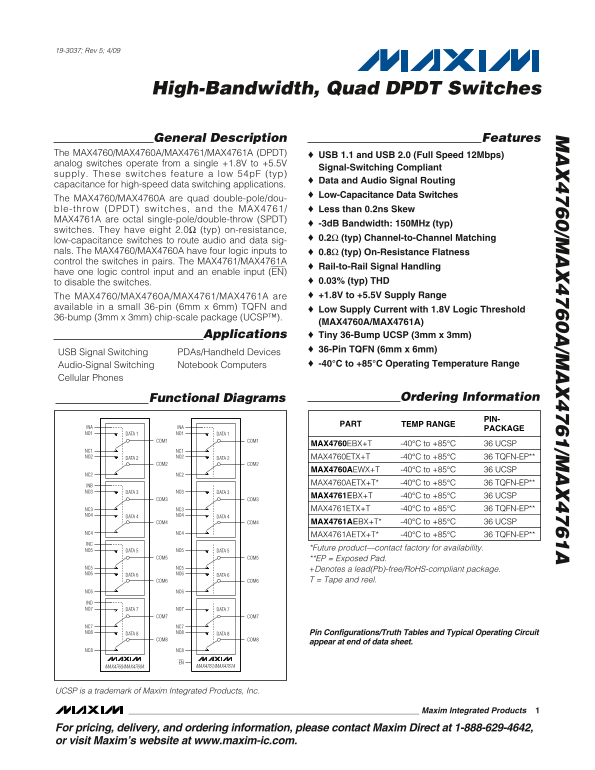
Page 1 Text Content
19-3037; Rev 5; 4/09
High-Bandwidth, Quad DPDT Switches
General Description Features
The MAX4760/MAX4760A/MAX4761/MAX4761A (DPDT) USB 1.1 and USB 2.0 (Full Speed 12Mbps) analog switches operate from a single +1.8V to +5.5V
Signal-Switching Compliant
supply. These switches feature a low 54p F (typ)
Data and Audio Signal Routing
capacitance for high-speed data switching applications.
Low-Capacitance Data Switches
The MAX4760/MAX4760A are quad double-pole/dou- ble-throw (DPDT) switches, and the MAX4761/ Less than 0.2ns Skew MAX4761A are octal single-pole/double-throw (SPDT)
-3d B Bandwidth: 150MHz (typ)
switches. They have eight 2.0Ω (typ) on-resistance,
0.2Ω (typ) Channel-to-Channel Matching
low-capacitance switches to route audio and data sig- nals. The MAX4760/MAX4760A have four logic inputs to 0.8Ω (typ) On-Resistance Flatness control the switches in pairs. The MAX4761/MAX4761A
Rail-to-Rail Signal Handling
have one logic control input and an enable input (EN)
to disable the switches. 0.03% (typ) THD The MAX4760/MAX4760A/MAX4761/MAX4761A are +1.8V to +5.5V Supply Range
available in a small 36-pin (6mm x 6mm) TQFN and
Low Supply Current with 1.8V Logic Threshold
36-bump (3mm x 3mm) chip-scale package (UCSP™).
(MAX4760A/MAX4761A) Applications Tiny 36-Bump UCSP (3mm x 3mm) 36-Pin TQFN (6mm x 6mm)
USB Signal Switching PDAs/Handheld Devices
Audio-Signal Switching Notebook Computers -40°C to +85°C Operating Temperature Range
Cellular Phones
Functional Diagrams Ordering Information
PART TEMP RANGE
INA INA
PACKAGE
NO1 DATA 1 NO1 DATA 1
COM1 COM1
MAX4760EBX+T -40°C to +85°C 36 UCSP
NC1 NC1 NO2 DATA 2 NO2 DATA 2 MAX4760ETX+T -40°C to +85°C 36 TQFN-EP**
COM2 COM2
MAX4760AEWX+T -40°C to +85°C 36 UCSP
NC2 NC2
MAX4760AETX+T* -40°C to +85°C 36 TQFN-EP**
INB NO3 DATA 3 NO3 DATA 3
MAX4761EBX+T -40°C to +85°C 36 UCSP
COM3 COM3
NC3 NC3 MAX4761ETX+T -40°C to +85°C 36 TQFN-EP** NO4 DATA 4 NO4 DATA 4
COM4 COM4 MAX4761AEBX+T* -40°C to +85°C 36 UCSP
NC4 NC4
MAX4761AETX+T* -40°C to +85°C 36 TQFN-EP**
NO5 DATA 5 NO5 *Future product—contact factory for availability.
DATA 5
COM5 COM5 **EP = Exposed Pad.
NC5 NC5
+Denotes a lead(Pb)-free/Ro HS-compliant package.
NO6 DATA 6 NO6 DATA 6
COM6 COM6 T = Tape and reel.
NC6 NC6
IND NO7 DATA 7 NO7 DATA 7
COM7 COM7
NC7 NC7 NO8 DATA 8 NO8 DATA 8 Pin Configurations/Truth Tables and Typical Operating Circuit
COM8 COM8
appear at end of data sheet.
NC8 NC8
EN MAX4760/MAX4760A MAX4761/MAX4761A
UCSP is a trademark of Maxim Integrated Products, Inc.
Maxim Integrated Products
For pricing, delivery, and ordering information, please contact Maxim Direct at 1-888-629-4642, or visit Maxim’s website at www.maxim-ic.com.
Page Summary Contents For MAXIM MAX4760 MAX4760A MAX4761 MAX4761A High-Bandwidth, Quad DPDT Switches
Manual Details
| Brand | QUAD |
|---|---|
| Pages | 14 |
| File Size | 228.43 KB |
| Published | May 31, 2026 |
Enter the captcha to get the download link:

Frequently Asked Questions
What are the key electrical characteristics of these switches?
They feature a -3dB Bandwidth of 150MHz (typ), eight 2.0Ω (typ) on-resistance, and low capacitance.
What temperature ranges can the MAX476x series handle?
The operational temperature range is specified from -40°C to +85°C.
In what types of electronic devices are these switches commonly used?
Applications include PDAs/Handheld Devices, Notebook Computers, dan Cellular Phones using USB Signal Switching.
What are the maximum ratings for soldering components?
Lead temperature (soldering) is +300°C, while the peak current when bumping is ±200mA.