MAXIM MAX4721 MAX4722 MAX4723 Dual SPST Analog Switches in UCSP Data Sheet
Summary
These compact dual SPST analog switches are engineered for reliable signal routing in low-voltage applications, operating seamlessly from +1.8V to +5.5V. Featuring low ON resistance and high bandwidth (>300MHz), they are perfect for USB 1.1 switching, audio data acquisition, and general-purpose circuit design. This manual provides comprehensive technical specifications, functional diagrams, package details (UCSP), and ordering guidance required for system integration by professional electronics engineers and designers.
Page 1 Text Content
19-2632; Rev 0; 10/02
4.5Ω Dual SPST Analog Switches in UCSP
General Description Features
The MAX4721/MAX4722/MAX4723 low-voltage, low on- USB 1.1 Signal Switching
resistance (RON), dual single-pole/single throw (SPST)
<2ns Differential Skew
analog switches operate from a single +1.8V to +5.5V
-3d B Bandwidth: >300MHz
supply. These devices are designed for USB 1.1 and
Low 15p F On-Channel Capacitance
audio switching applications.
Low RON (max) Switches
The MAX4721/MAX4722/MAX4723 feature 4.5Ω RON
4.5Ω (max) (+3V Supply)
(max) with 1.2Ω flatness and 0.3Ω matching between
3Ω (max) (+5V Supply)
channels. These new switches feature guaranteed
operation from +1.8V to +5.5V and are fully specified at 0.3Ω (max) RON Match (+3V Supply)
3V and 5V. These switches offer break-before-make
1.2Ω (max) RON Flatness (+3V Supply)
switching (1ns) with t ON <80ns and t OFF <40ns at
<0.5n A Leakage Current at TA = +25°C
+2.7V. The digital logic inputs are +1.8V logic compati-
ble with a +2.7V to +3.6V supply. High Off-Isolation: -55d B (10MHz) Low Crosstalk: -80d B (10MHz)
These switches are packaged in a chip-scale package (UCSP™), significantly reducing the required PC board Low Distortion: 0.03% area. The chip occupies only a 1.52mm ✕ 1.52mm area
+1.8V CMOS-Logic Compatible
and has a 3 ✕ 3 bump array with a bump pitch of
Single-Supply Operation from +1.8V to +5.5V
0.5mm. These switches are also available in an 8-pin
µMAX package. Rail-to-Rail® Signal Handling
Applications Ordering Information
Battery-Operated Equipment PIN/BUMP-
PART TEMP RANGE
PACKAGE MARK
Audio/Video-Signal Routing
MAX4721EUA -40°C to +85°C 8 µMAX
Low-Voltage Data-Acquisition Systems
MAX4721EBL-T* -40°C to +85°C 9 UCSP-9 ABP
Sample-and-Hold Circuits
MAX4722EUA -40°C to +85°C 8 µMAX
Communications Circuits
MAX4722EBL-T* -40°C to +85°C 9 UCSP-9 ABQ MAX4723EUA -40°C to +85°C 8 µMAX MAX4723EBL-T* -40°C to +85°C 9 UCSP-9 ABR Note: UCSP package requires special solder temperature pro- file described in the Absolute Maximum Ratings section. *UCSP reliability is integrally linked to the user’s assembly meth- ods, circuit board material, and environment. See the UCSP reli-
Rail-to-Rail is a registered trademark of Nippon Motorola, Ltd.
ability notice in the UCSP Reliability section of this data sheet for
UCSP is a trademark of Maxim Integrated Products, Inc.
more information.
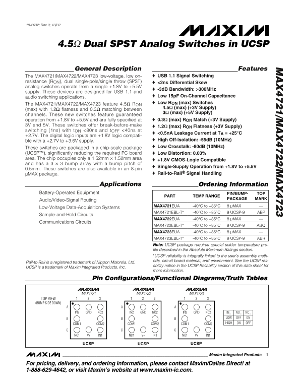
Pin Configurations/Functional Diagrams/Truth Tables
MAX4721 MAX4722 MAX4723
TOP VIEW (BUMP SIDE DOWN)
IN2 GND NO2 IN2 GND NC2 IN2 GND NC2 IN_ NO_ NC_
LOW OFF ON COM1 COM2 COM1 COM2 COM1 COM2 HIGH ON OFF
NO1 V+ IN1 NC1 V+ IN1 NO1 V+ IN1
UCSPUCSP UCSP
Maxim Integrated Products
For pricing, delivery, and ordering information, please contact Maxim/Dallas Direct! at 1-888-629-4642, or visit Maxim’s website at www.maxim-ic.com.
Page Summary Contents For MAXIM MAX4721 MAX4722 MAX4723 Dual SPST Analog Switches in UCSP Data Sheet
Manual Details
| Brand | Dual |
|---|---|
| Pages | 14 |
| File Size | 293.33 KB |
| Published | June 06, 2026 |
Enter the captcha to get the download link:

Frequently Asked Questions
What is the operating voltage range for these analog switches?
They operate from a single +1.8V to +5.5V, supporting low-voltage data and signal routing.
How high is the maximum On-Resistance (R_ON)?
The devices feature 4.5Ω R(ON) max with excellent linearity and low matching at specified voltages.
What are common application areas for these switches?
They are designed for USB 1.1 signaling, audio/video signal routing, and general data-acquisition applications.
What specific soldering precautions must be taken for the UCSP package?
The UCSP package requires a special solder temperature profile (JEDEC 020A) with warning that hand or wave soldering is not allowed.