LINEAR Tiny Versatile Buck Regulators - Operation from 3.6V to 36V Input Design Note 367 Data Sheet User Manual
Summary
Explore maximum efficiency with the LT1936 and LT1933 step-down buck regulators, engineered for demanding systems requiring robust stable power delivery from 3.6V to 36V input. This manual provides comprehensive application details for generating complex voltages, including negative outputs and powering multiple loads from extremely low supplies (down to 4.5V). Ideal for professional designers working on space-constrained or mission-critical industrial and automotive electronics that require maximum versatility and high component reliability.
Page 1 Text Content
advertisement
Tiny Versatile Buck Regulators Operate from 3.6V to 36V Input Design Note 367 Hua (Walker) Bai
Introduction extends battery life in applications that spend long periods of time in sleep or shutdown mode. During short circuit,
Linear Technology offers two new buck regulators that
both parts offer frequency foldback, where the switching
operate from a wide input voltage range (3.6V to 36V) and
frequency decreases by about a factor of ten. The lower
take so little space that they easily solve many difficult
frequency allows the inductor current to safely discharge,
power supply problems. The LT®1936 and LT1933 are
thereby preventing current runaway.
perfect for applications with disparate power inputs or wide range input power supplies such as automotive
LT1936 Produces 3.3V at 1.2A from 4.5V to 36V
batteries, 24V industrial supplies, 5V logic supplies and
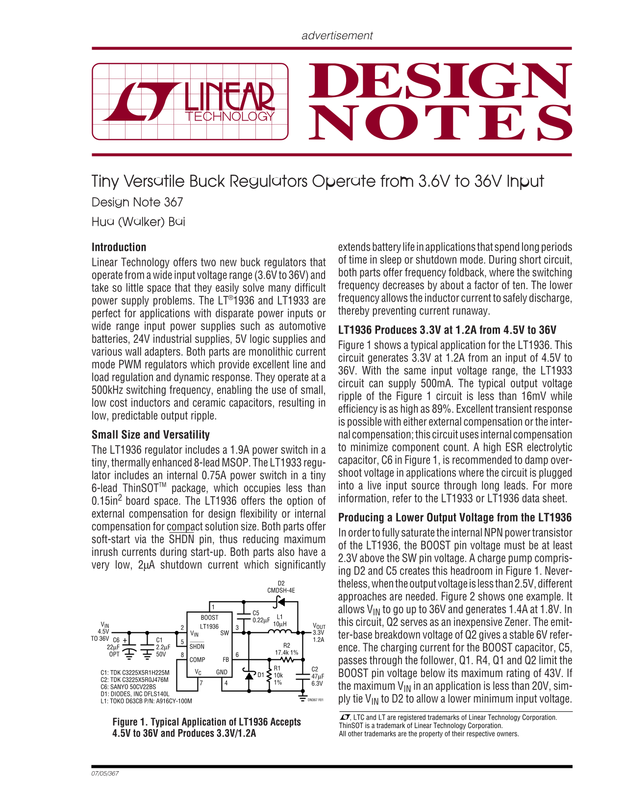
Figure 1 shows a typical application for the LT1936. This
various wall adapters. Both parts are monolithic current
circuit generates 3.3V at 1.2A from an input of 4.5V to
mode PWM regulators which provide excellent line and
36V. With the same input voltage range, the LT1933
load regulation and dynamic response. They operate at a
circuit can supply 500m A. The typical output voltage
500k Hz switching frequency, enabling the use of small,
ripple of the Figure 1 circuit is less than 16m V while
low cost inductors and ceramic capacitors, resulting in
efficiency is as high as 89%. Excellent transient response
low, predictable output ripple.
is possible with either external compensation or the inter- Small Size and Versatility nal compensation; this circuit uses internal compensation to minimize component count. A high ESR electrolytic
The LT1936 regulator includes a 1.9A power switch in a
capacitor, C6 in Figure 1, is recommended to damp over-
tiny, thermally enhanced 8-lead MSOP. The LT1933 regu-
shoot voltage in applications where the circuit is plugged
lator includes an internal 0.75A power switch in a tiny
into a live input source through long leads. For more
6-lead Thin SOTTM package, which occupies less than
0.15in2 board space. The LT1936 offers the option of information, refer to the LT1933 or LT1936 data sheet.
external compensation for design flexibility or internal
Producing a Lower Output Voltage from the LT1936
compensation for compact solution size. Both parts offer
In order to fully saturate the internal NPN power transistor
soft-start via the SHDN pin, thus reducing maximum
of the LT1936, the BOOST pin voltage must be at least
inrush currents during start-up. Both parts also have a
2.3V above the SW pin voltage. A charge pump compris-
very low, 2µA shutdown current which significantly
ing D2 and C5 creates this headroom in Figure 1. Never-
D2 theless, when the output voltage is less than 2.5V, different CMDSH-4E
approaches are needed. Figure 2 shows one example. It allows VIN to go up to 36V and generates 1.4A at 1.8V. In
C5 BOOST L1 0.22µF
VIN 10µH VOUT this circuit, Q2 serves as an inexpensive Zener. The emit-
LT1936
4.5V VIN SW 3.3V
ter-base breakdown voltage of Q2 gives a stable 6V refer-
TO 36V C6 C1 1.2A
22µF 2.2µF SHDN R2
ence. The charging current for the BOOST capacitor, C5,
OPT 50V 17.4k 1%
COMP FB passes through the follower, Q1. R4, Q1 and Q2 limit the
C1: TDK C3225X5R1H225M VC GND
D1 10k 47µF BOOST pin voltage below its maximum rating of 43V. If
C2: TDK C3225X5R0J476M
C6: SANYO 50CV22BS the maximum VIN in an application is less than 20V, sim- D1: DIODES, INC DFLS140L
DN367 F01 ply tie VIN to D2 to allow a lower minimum input voltage.
L1: TOKO D63CB P/N: A916CY-100M
, LTC and LT are registered trademarks of Linear Technology Corporation.
Figure 1. Typical Application of LT1936 Accepts
Thin SOT is a trademark of Linear Technology Corporation. 4.5V to 36V and Produces 3.3V/1.2A All other trademarks are the property of their respective owners.
Page Summary Contents For LINEAR Tiny Versatile Buck Regulators - Operation from 3.6V to 36V Input Design Note 367 Data Sheet User Manual
Manual Details
| Brand | Linear |
|---|---|
| Pages | 2 |
| File Size | 64.36 KB |
| Published | July 16, 2026 |
Enter the captcha to get the download link:

Frequently Asked Questions
What is the wide input voltage range for these regulators?
They operate from a wide input voltage range of 3.6V to 36V.
What type of current switch does the LT1936 include?
The LT1936 regulator includes a 1.9A power switch in its package.
Can these regulators handle negative output voltages?
Yes, Figure 3 shows one example where the circuit generates -3.3V from a minimum 4.5V supply.
What efficiency can the LT1933 achieve?
The LT1933 can achieve an efficiency as high as 89%.