LINEAR SYSTEMS LS840 LS841 LS842 DATASHEET
Summary
These low noise, low drift, low capacitance monolithic dual N-channel JFET transistors deliver exceptionally stable and clean signal performance. Ideal for audiophile and sensitive electronic applications requiring high fidelity signal transmission. This documentation provides comprehensive electrical characteristics, absolute maximum ratings, and technical data necessary for reliable circuit design and engineering implementation. Designed for professional engineers needing superior performance in critical amplifier or signal processing circuits.
Page 1 Text Content
LS840 LS841 LS842 LOW NOISE LOW DRIFT LOW CAPACITANCE
Linear Integrated Systems
MONOLITHIC DUAL N-CHANNEL JFET
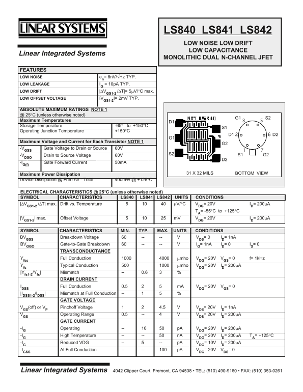
FEATURES LOW NOISE en= 8n V/√Hz TYP. LOW LEAKAGE IG = 10p A TYP. LOW DRIFT |∆VGS1-2 /∆T|= 5µV/°C max. LOW OFFSET VOLTAGE IVGS1-2I= 2m V TYP.
ABSOLUTE MAXIMUM RATINGS NOTE 1 @ 25°C (unless otherwise noted)
Maximum Temperatures
Storage Temperature -65° to +150°C
Operating Junction Temperature +150°C
Maximum Voltage and Current for Each Transistor NOTE 1
-VGSS Gate Voltage to Drain or Source 60V
-VDSO Drain to Source Voltage 60V
-IG(f) Gate Forward Current 50m A
31 X 32 MILS BOTTOM VIEW
Maximum Power Dissipation Device Dissipation @ Free Air - Total 400m W @ +125°C
ELECTRICAL CHARACTERISTICS @ 25°C (unless otherwise noted) SYMBOL CHARACTERISTICS LS840 LS841 LS842 UNITS CONDITIONS
|∆VGS1-2 /∆T| max. Drift vs. Temperature µV/°C VDG= 20V ID= 200µA
TA= -55°C to +125°C
|VGS1-2| max. Offset Voltage m V VDG= 20V ID= 200µA
SYMBOL CHARACTERISTICS MIN. TYP. MAX. UNITS CONDITIONS
BVGSS Breakdown Voltage VDS= 0 ID= 1n A
BVGGO Gate-to-Gate Breakdown IG= 1n A ID= 0 IS= 0
TRANSCONDUCTANCE Yfss Full Conduction µmho VDG= 20V VGS= 0 f= 1k Hz Yfs Typical Conduction µmho VDG= 20V ID= 200µA
|Yfs1-2/Yfs| Mismatch 0.6
DRAIN CURRENT IDSS Full Conduction 0.5 m A VDG= 20V VGS= 0
|IDSS1-2/IDSS| Mismatch at Full Conduction
GATE VOLTAGE
VGS(off) or VP Pinchoff Voltage 4.5 VDS= 20V ID= 1n A VGS Operating Range 0.5 VDS= 20V ID= 200µA
GATE CURRENT -IG Operating p A VDG= 20V ID= 200µA
-IG High Temperature n A VDG= 20V ID= 200µA TA= +125°C -IG Reduced VDG p A VDG= 10V ID= 200µA -IGSS At Full Conduction p A VDG= 20V VDS= 0
Linear Integrated Systems 4042 Clipper Court, Fremont, CA 94538 • TEL: (510) 490-9160 • FAX: (510) 353-0261
Page Summary Contents For LINEAR SYSTEMS LS840 LS841 LS842 DATASHEET
Manual Details
| Brand | Linear |
|---|---|
| Pages | 2 |
| File Size | 32.58 KB |
| Published | June 17, 2026 |
Enter the captcha to get the download link:

Frequently Asked Questions
What is the maximum power dissipation for this device?
Total dissipation at free air is 400mW @ +125°C.
What is the typical low drop/leakage current (I)?
The typical leakage current (I) is 10pA.
Can the product withstand high temperatures?
It has an absolute maximum junction temperature (Tj) of +150°C, and the storage temperature range is -65° to +150°C.