LINEAR LTC3406 Data Sheet
Summary
Design your compact, high-performance electronics with the LTC3406 synchronous step-down regulator. Offering up to 96% efficiency and ultra-low quiescent current (as low as ≤1µA), this device ensures extended battery life for portable applications. The manual provides comprehensive specifications, detailing its constant 1.5MHz operation, low dropout capability using a dedicated 0.6V reference, and suitability for Li-Ion battery systems. Ideal for designers of cellular equipment, wireless modems, and digital cameras requiring reliable power in minimal ThinSOT packages.
Page 1 Text Content
查询LTC3406-1.5供应商
LTC3406
LTC3406-1.5/LTC3406-1.8 1.5MHz, 600m A Synchronous Step-Down Regulator in Thin SOT
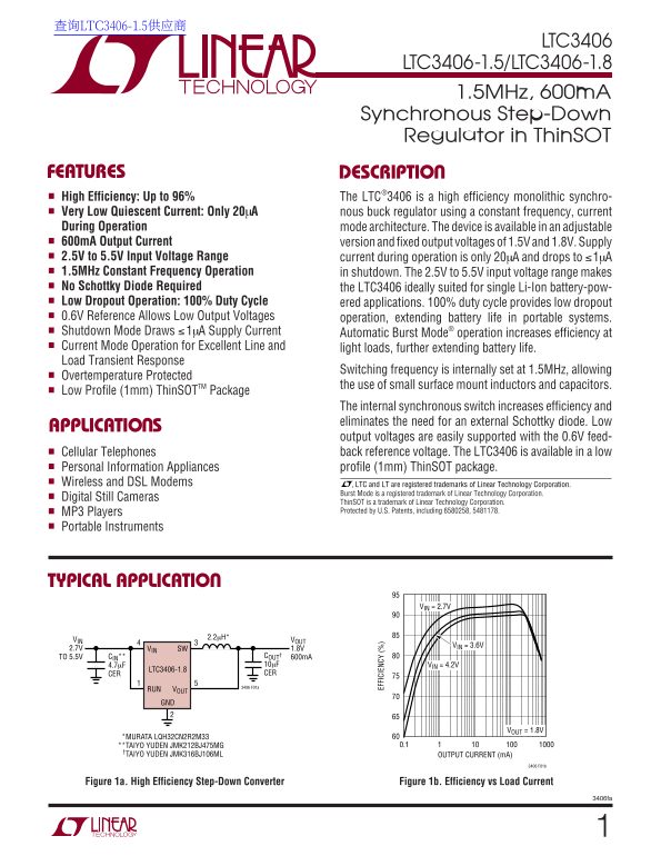
FEATURES DESCRIPTIO High Efficiency: Up to 96% The LTC®3406 is a high efficiency monolithic synchro- Very Low Quiescent Current: Only 20µA nous buck regulator using a constant frequency, current During Operation mode architecture. The device is available in an adjustable 600m A Output Current version and fixed output voltages of 1.5V and 1.8V. Supply 2.5V to 5.5V Input Voltage Range current during operation is only 20µA and drops to ≤1µA 1.5MHz Constant Frequency Operation in shutdown. The 2.5V to 5.5V input voltage range makes No Schottky Diode Required the LTC3406 ideally suited for single Li-Ion battery-pow- Low Dropout Operation: 100% Duty Cycle ered applications. 100% duty cycle provides low dropout 0.6V Reference Allows Low Output Voltages operation, extending battery life in portable systems. Shutdown Mode Draws ≤1µA Supply Current Automatic Burst Mode® operation increases efficiency at Current Mode Operation for Excellent Line and light loads, further extending battery life. Load Transient Response
Switching frequency is internally set at 1.5MHz, allowing
Overtemperature Protected
EF FI CI EN CY
the use of small surface mount inductors and capacitors.
Low Profile (1mm) Thin SOTTM Package
The internal synchronous switch increases efficiency and eliminates the need for an external Schottky diode. Low
APPLICATIO S
output voltages are easily supported with the 0.6V feed- Cellular Telephones back reference voltage. The LTC3406 is available in a low Personal Information Appliances profile (1mm) Thin SOT package.
Wireless and DSL Modems , LTC and LT are registered trademarks of Linear Technology Corporation.
Burst Mode is a registered trademark of Linear Technology Corporation.
Digital Still Cameras
Thin SOT is a trademark of Linear Technology Corporation. MP3 Players Protected by U.S. Patents, including 6580258, 5481178.
Portable Instruments
TYPICAL APPLICATIO
VIN = 2.7V
VIN VOUT
VIN = 3.6V
2.7V VIN SW 1.8V
TO 5.5V CIN** COUT† 600m A 4.7µF 10µF VIN = 4.2V
LTC3406-1.8
CER CER 3406 F01a
RUN VOUT GND
VOUT = 1.8V
MURATA LQH32CN2R2M33
TAIYO YUDEN JMK212BJ475MG 0.1
TAIYO YUDEN JMK316BJ106ML OUTPUT CURRENT (m A)
Figure 1a. High Efficiency Step-Down Converter Figure 1b. Efficiency vs Load Current
3406fa
Page Summary Contents For LINEAR LTC3406 Data Sheet
Manual Details
| Brand | Linear |
|---|---|
| Pages | 16 |
| File Size | 231.67 KB |
| Published | June 17, 2026 |
Enter the captcha to get the download link:

Frequently Asked Questions
What is the operating temperature range for this regulator?
The operational temperature range is from –40°C to 85°C.
How low can the device drop current draw in standby mode?
In shutdown mode, the supply current draws less than or equal to 1µA.
Does the LTC3406 require an external Schottky diode?
No, the internal synchronous switch eliminates the need for an external Schottky diode.
What is the maximum safe input voltage range?
The device supports an input supply voltage between –0.3V and 6V.