LINEAR LTC3100 User Guide
Summary
This highly efficient, multichannel DC/DC converter simplifies complex power design for sensitive electronics. It is ideal for portable medical devices and consumer products that require multiple low-noise outputs (like 3.3V and 1.8V) from varied sources, including USB, wall adapters, or single/multiple batteries down to 0.7V. The manual details how this compact device ensures stable voltage sequencing through sophisticated features like an integrated LDO and automatic Burst Mode operation.
Page 1 Text Content
L DESIGN IDEAS
Multi-Rail DC/DC Converter in a 3mm × 3mm QFN Takes
Inputs as Low as 0.7V by Dave Salerno
Introduction
MBR0520 Modern handheld instrumentation, USB 3.3V AT: 100m A FOR VBATT = 1.2V INPUT 300m A FOR VBATT = 2.4V
portable medical devices and con-
4.7µF 250m A FOR USB INPUT 3.3µH
sumer electronics demand a multitude
VBATT
of power rails for internal processors, 4.7µF
0.9V TO 1.07M
SWBST VINBK VBST
memory, audio and color displays.
VINBST FBBST
EF FI CI EN CY
Popular battery technologies for these 4.7µF 324k
devices include single or multiple VLDO
cell alkaline, Ni MH or Li-Poly/Li-Ion 301k
LTC3100
batteries. Operation from a USB port FBLDO
1.8V AT 50m A
or a wall adapter is another common 100k
trait. Replaceable alkaline batteries 2.2µF
are particularly attractive for remote 10µH
MODE SWBK
locations and portable medical devices
where power or time is not available RUNBST FBBK
to recharge batteries. The challenge RUNLDO PGBST is to create a compact and efficient
RUNBK GND PGBK
power solution for these wide VIN
range, multi-output applications. The LTC3100 multichannel DC/DC converter makes it easier to meet this
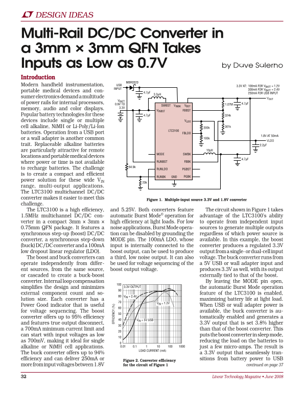
Figure 1. Multiple-input source 3.3V and 1.8V converter
challenge. The LTC3100 is a high efficiency, and 5.25V. Both converters feature The circuit shown in Figure 1 takes 1.5MHz multichannel DC/DC con- automatic Burst Mode® operation for advantage of the LTC3100’s ability verter in a compact 3mm × 3mm × high efficiency at light loads. For low to operate from independent input 0.75mm QFN package. It features a noise applications, Burst Mode opera- sources to generate multiple outputs synchronous step-up (boost) DC/DC tion can be disabled by grounding the regardless of which power source is converter, a synchronous step-down MODE pin. The 100m A LDO, whose available. In this example, the boost (buck) DC/DC converter and a 100m A input is internally connected to the converter produces a regulated 3.3V low dropout linear regulator (LDO). boost output, can be used to produce output from a single- or dual-cell input The boost and buck converters can a third, low noise output. It can also voltage. The buck converter runs from operate independently from differ- be used for voltage sequencing of the a 5V USB or wall adapter input and ent sources, from the same source, boost output voltage. produces 3.3V as well, with its output or cascaded to create a buck-boost externally tied to that of the boost. converter. Internal loop compensation By leaving the MODE pin open,
simplifies the design and minimizes 3.3V OUTPUT the automatic Burst Mode operation
external component count and so- feature of the LTC3100 is enabled,
VIN = 2.4V
lution size. Each converter has a maximizing battery life at light load.
VIN = 1.2V
Power Good indicator that is useful When USB or wall adapter power is for voltage sequencing. The boost available, the buck converter is au- converter offers up to 95% efficiency tomatically enabled and generates a
VIN = 5V USB
and features true output disconnect, 3.3V output that is set 3.8% higher a 700m A minimum current limit and than that of the boost converter. This can start with input voltages as low puts the boost converter in sleep mode, as 700m V, making it ideal for single reducing the load on the batteries to
alkaline or Ni MH cell applications. 0.01 0.1 just a few micro-amps. The result is
LOAD CURRENT (m A)
The buck converter offers up to 94% a 3.3V output that seamlessly tran- efficiency and can deliver 250m A or sitions from battery power to USB
Figure 2. Converter efficiency
more from input voltages between 1.8V for the circuit of Figure 1 continued on page 37
Linear Technology Magazine • June 2008
Page Summary Contents For LINEAR LTC3100 User Guide
Manual Details
| Brand | Linear |
|---|---|
| Pages | 2 |
| File Size | 295.47 KB |
| Published | June 15, 2026 |
Enter the captcha to get the download link:

Frequently Asked Questions
What is the package size of the LTC3100?
It comes in a 3mm × 3mm × 0.75mm QFN package.
What is the minimum input voltage for the boost converter?
The boost converter can start with input voltages as low as 700mV.
How do you disable Burst Mode operation?
Ground the MODE pin to disable Burst Mode operation.
What is the maximum current the LDO can deliver?
The LDO can deliver up to 100mA of current.