LINEAR LTC3612 User Guide
Summary
The LTC3612 is a compact, high-efficiency monolithic synchronous buck regulator designed for robust power delivery across varying loads. It features a wide input voltage range (suitable for Li-Ion batteries) and offers multiple operating modes—including Burst Mode, Pulse Skipping, and Forced Continuous—to optimize performance without sacrificing efficiency. This manual provides detailed technical guidance on configuring its constant frequency switching, transient response handling, and power good indicator functionality. Ideal for electronics designers building space-constrained, high-performance applications requiring reliable, adjustable voltage regulation down to 0.6V.
Page 1 Text Content
L DESIGN FEATURES
Monolithic Synchronous Step-Down Regulator Sources 3A or Sinks 1.5A in TSSOP or 3mm × 4mm QFN
by Genesia Bertelle
Introduction
The LTC3612 monolithic synchronous
buck regulator can source 3A and
SVIN PVIN
sink 1.5A from a tiny 3mm × 4mm
RUN PWN_DRIVER
QFN or 20-lead TSSOP package with 402k
EF FI CI EN CY TRACKSS DDR
exposed pads for improved thermal
VTT=VDD/2
performance. This device saves space, RT_SYNC SW 1.25V
LT3612 L1
minimizes external components and is
highly efficient. It employs a constant PGOOD SGROUND
frequency, current mode architecture ITH
PGROUND
that operates from an input range of
1M 470p F 10p F MODE VFB
2.25V to 5.5V—suitable for a single 165k
Li-Ion battery or low voltage input
applications. The LTC3612 provides
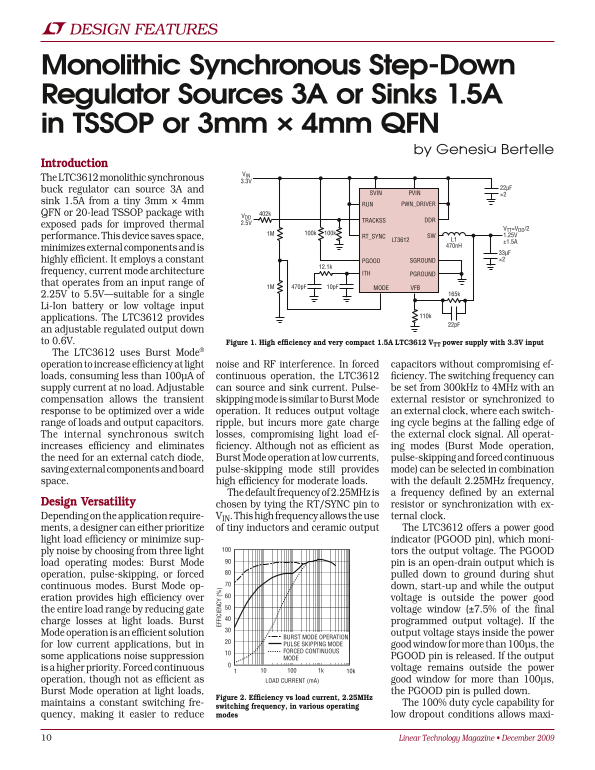
an adjustable regulated output down to 0.6V. Figure 1. High efficiency and very compact 1.5A LTC3612 VTT power supply with 3.3V input The LTC3612 uses Burst Mode® operation to increase efficiency at light noise and RF interference. In forced capacitors without compromising ef- loads, consuming less than 100µA of continuous operation, the LTC3612 ficiency. The switching frequency can supply current at no load. Adjustable can source and sink current. Pulse- be set from 300k Hz to 4MHz with an compensation allows the transient skipping mode is similar to Burst Mode external resistor or synchronized to response to be optimized over a wide operation. It reduces output voltage an external clock, where each switch- range of loads and output capacitors. ripple, but incurs more gate charge ing cycle begins at the falling edge of The internal synchronous switch losses, compromising light load ef- the external clock signal. All operat- increases efficiency and eliminates ficiency. Although not as efficient as ing modes (Burst Mode operation, the need for an external catch diode, Burst Mode operation at low currents, pulse-skipping and forced continuous saving external components and board pulse-skipping mode still provides mode) can be selected in combination space. high efficiency for moderate loads. with the default 2.25MHz frequency,
The default frequency of 2.25MHz is a frequency defined by an external
Design Versatility chosen by tying the RT/SYNC pin to resistor or synchronization with ex- Depending on the application require- VIN. This high frequency allows the use ternal clock. ments, a designer can either prioritize of tiny inductors and ceramic output The LTC3612 offers a power good light load efficiency or minimize sup- indicator (PGOOD pin), which moni- ply noise by choosing from three light tors the output voltage. The PGOOD load operating modes: Burst Mode pin is an open-drain output which is operation, pulse-skipping, or forced pulled down to ground during shut continuous modes. Burst Mode op- down, start-up and while the output eration provides high efficiency over voltage is outside the power good the entire load range by reducing gate voltage window (±7.5% of the final charge losses at light loads. Burst programmed output voltage). If the Mode operation is an efficient solution output voltage stays inside the power
BURST MODE OPERATION for low current applications, but in PULSE SKIPPING MODE good window for more than 100µs, the FORCED CONTINUOUS
some applications noise suppression MODE PGOOD pin is released. If the output is a higher priority. Forced continuous 1k voltage remains outside the power
operation, though not as efficient as LOAD CURRENT (m A) good window for more than 100µs, Burst Mode operation at light loads, the PGOOD pin is pulled down.
Figure 2. Efficiency vs load current, 2.25MHz
maintains a constant switching fre- The 100% duty cycle capability for
switching frequency, in various operating
quency, making it easier to reduce modes low dropout conditions allows maxi-
Linear Technology Magazine • December 2009
Page Summary Contents For LINEAR LTC3612 User Guide
Manual Details
| Brand | Linear |
|---|---|
| Pages | 3 |
| File Size | 564.25 KB |
| Published | June 03, 2026 |
Enter the captcha to get the download link:

Frequently Asked Questions
What kind of Regulator sources can the LTC3612 handle?
It is a monolithic synchronous step-down regulator that can source up to 3A and sink up to 1.5A.
How does the device maintain efficiency at light loads?
It uses Burst Mode operation, pulse-skipping mode, and forced continuous mode to increase efficiency by reducing gate charge losses.
What are the benefits of adjustable output voltage regulation?
The LTC3612 provides regulated output down to 0.6V for various applications like powering DDR memory or battery charging.
Is there a power good indicator?
Yes, it has a PGOOD pin that is an open-drain output used to monitor when the output voltage remains within the specified 'power good' operating window.