LINEAR LTC2274 User Guide
Summary
This design features article from Linear Technology presents the LTC2274 105 Msps 16-bit ADC, which replaces the traditional parallel interface with a novel high-speed serial interface using 8B/10B encoding and current mode logic signaling at 2.1 Gbps over a single self-clocking differential pair. The serial interface reduces the required data I/O lines from 16 CMOS or 32 LVDS parallel lines to just one differential pair, freeing FPGA pins and board space while providing an effective isolation b
Page 1 Text Content
DESIGN FEATURES L
AM PL IT (d BF S)
Serial Interface for High Speed Data Converters Simplifies Layout over Traditional Parallel Devices
by Clarence Mayott
Introduction The LTC2274 is a 105Msps, 16-bit signaling uses current mode logic ADC that simplifies the digital connec- The LTC2274 ADC replaces (CML), which is capable of transmitting tion between the ADC and FPGA by data in excess of 10GHz.
the usual parallel interface
replacing the usual parallel interface Current mode logic uses a differ-
with a novel high speed
with a novel high speed serial interface, ential output transistor pair (usually
serial interface, thus
thus reducing the typical number of N-type) to steer current into resistive
reducing the typical number
required data input/output (I/O) lines loads. The output swing and offset
from 16 CMOS or 32 LVDS parallel of required data input/ depends on the bias current and
data lines to a single, self-clocking, output lines from 16 CMOS termination resistance. The output differential pair communicating at driver bias current is typically 16m A,
or 32 LVDS to a single, self-
2.1Gbps. This frees up valuable FPGA generating a signal swing potential
clocking, differential pair
pins and board space. It also allows of 400m VP–P (800m VP–P differential)
communicating at 2.1Gbps.
flexibility to route across analog and across the combined internal and digital boundaries—in noise sensi- external termination resistance of 25Ω tive applications, the serial interface and achieves similar AC performance. on each output. LVDS typically uses provides an effective isolation barrier However, the LTC2274 differs from the 3.5m A to develop its signal swing, and between digital and analog circuitry LTC2207 in its output structure. The the capacitance of the ESD protection and serves to eliminate coupling be- LTC2274 uses an 8B/10B encoder to diodes becomes a limiting factor for tween the digital outputs and analog encode and serialize the data before it transmission speed. CML uses more
BI ER RO RA TE (B ER
inputs to reduce digital feedback. is transmitted. 8B/10B encoding is a current, and therefore this capacitance
process that takes 8 bits of data and becomes less of a limiting factor to
Current Mode Logic and
encodes them into 10 bits to ensure data throughput.
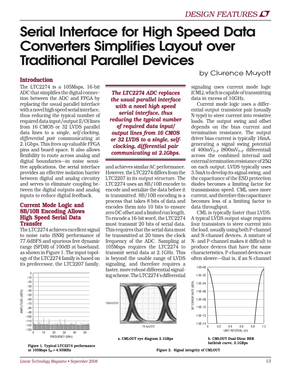
8B/10B Encoding Allows zero DC offset and a limited run length. CML is typically faster than LVDS. High Speed Serial Data To encode a 16-bit word, the LTC2274 A typical LVDS output stage requires Transfer must transmit 20 bits of serial data. four transistors to steer current into The LTC2274 achieves excellent signal This requires that the serial data must the load, usually using both P-channel to noise ratio (SNR) performance of be transmitted at 20 times the clock and N-channel devices. A mixture of 77.6d BFS and spurious free dynamic frequency of the ADC. Sampling at N- and P-channel makes it difficult to range (SFDR) of 100d B at baseband, 105Msps requires the LTC2274 to produce devices that have the same as shown in Figure 1. The input topol- transmit serial data at 2.1GHz. This characteristics. P-channel devices are ogy of the LTC2274 family is based on is beyond the usable range of LVDS often slower—that is, if an N-channel its predecessor, the LTC2207 family, signaling, and therefore requires a
faster, more robust differential signal-
ing scheme. The LTC2274’s differential 1.0E–02
–70 100m V/DIV
79.4ps/DIV 0.80.4 1.00.60.2
–130 UNIT INTERVAL (UI)
FREQUENCY (MHz)
a. CMLOUT eye diagram 2.1GBps b. CMLOUT Dual-Dirac BER
bathtub curve, 2.1GBps
Figure 1. Typical LTC2274 performance at 105Msps f IN = 4.93MHz Figure 2. Signal integrity of CMLOUT
Linear Technology Magazine • September 2008
Page Summary Contents For LINEAR LTC2274 User Guide
Manual Details
| Brand | Linear |
|---|---|
| Pages | 3 |
| File Size | 407.05 KB |
| Published | June 18, 2026 |
Enter the captcha to get the download link:

Frequently Asked Questions
What does CML stand for and what is its key advantage over LVDS?
CML stands for Current Mode Logic. Its key advantage is improved signal integrity because it only sinks current, making it faster than traditional signaling methods like LVDS.
How large of a data transfer rate can the LTC2274 achieve?
The LTC2274 can transmit serial data at 2.1 Gbps while sampling at 105 Msps.
What is used to ensure clean signal transmission in the LTC2274's output structure?
It uses an 8B/10B encoder, a process that encodes every 8 bits of data into 10 bits to maintain continuous signaling and prevent DC offset.
How does the PMIC simplify power supply control for design?
Modern PMICs allow designers to program complex power-up sequences in fewer ICs via pin-strapping, simplifying board layout and increasing flexibility compared to traditional solutions.