LINEAR LTC2262 User Guide
Summary
The LTC2262 family provides advanced, ultralow-power Analog-to-Digital Converters (ADCs) up to 150Msps. Engineered for applications like base stations and portable electronics, these ADCs significantly reduce power dissipation while maintaining superior AC performance. The manual details various low-power modes, including DDR CMOS and LVDS signaling, simplifying circuit design by minimizing data lines and improving thermal efficiency across single and multi-channel configurations.
Page 1 Text Content
DESIGN FEATURES L
New Generation of 14-Bit 150Msps ADCs Dissipates a Third the Power of the Previous Generation without Sacrificing AC Performance
by Clarence Mayott Introduction
The LTC2262 family of ultralow power, where high temperatures can degrade
high speed analog-to-digital convert- SNR.
–20 AM PL IT UD (d BF S)
ers dissipates less than one third the
power of comparable earlier-genera- Digital Outputs
–40 tion ADCs while maintaining excellent –50 The LTC2262 family also offers some –60
AC performance. Ultralow power unique digital features to simplify
makes it possible to add features to and overall design in a wide variety of
improve the performance of power- applications. The LTC2262 can be
limited applications while remaining –100 configured to run in one of three data
within the power budget. Of course, –110 output modes: full rate CMOS, double –120
improved operating efficiency also data rate (known as DDR) CMOS, and
FREQUENCY (MHz)
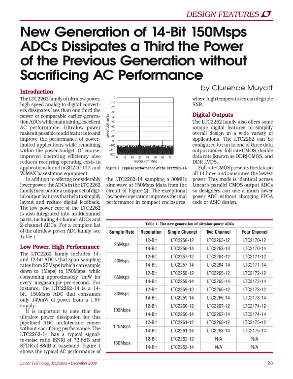
reduces recurring operating costs in DDR LVDS. applications found in 3G/4G LTE and Figure 1. Typical performance of the LTC2262-14 Full rate CMOS presents the data on Wi MAX basestation equipment. all 14 lines and consumes the lowest In addition to offering considerably the LTC2262-14 sampling a 30MHz power. This mode is identical across lower power, the ADCs in the LTC2262 sine wave at 150Msps (data from the Linear’s parallel CMOS output ADCs family incorporate a unique set of digi- circuit of Figure 2). The exceptional so designers can use a much lower tal output features that help to simplify low power operation improves thermal power ADC without changing FPGA layout and reduce digital feedback. performance in compact enclosures, code or ASIC design. The low power core of the LTC2262 is also integrated into multichannel parts, including 4-channel ADCs and
Table 1. The new generation of ultralow-power ADCs
2-channel ADCs. For a complete list of the ultralow-power ADC family, see Sample Rate Resolution Single Channel Two Channel Four Channel Table 1.
12-Bit LTC2256-12 LTC2263-12 LTC2170-12
25Msps
Low Power, High Performance
14-Bit LTC2256-14 LTC2263-14 LTC2170-14
The LTC2262 family includes 14-
12-Bit LTC2257-12 LTC2264-12 LTC2171-12
and 12-bit ADCs that span sampling 40Msps
rates from 25Msps (which can sample 14-Bit LTC2257-14 LTC2264-14 LTC2171-14
down to 1Msps) to 150Msps, while
12-Bit LTC2258-12 LTC2265-12 LTC2172-12
consuming approximately 1m W for 65Msps
14-Bit LTC2258-14 LTC2265-14 LTC2172-14
every megasample-per-second. For instance, the LTC2262-14 is a 14-
12-Bit LTC2259-12 LTC2266-12 LTC2173-12
bit, 150Msps ADC that consumes 80Msps
14-Bit LTC2259-14 LTC2266-14 LTC2173-14
only 149m W of power from a 1.8V supply. 12-Bit LTC2260-12 LTC2267-12 LTC2174-12
105Msps
It is important to note that the
14-Bit LTC2260-14 LTC2267-14 LTC2174-14
ultralow power dissipation for this
pipelined ADC architecture comes 12-Bit LTC2261-12 LTC2268-12 LTC2175-12
125Msps
without sacrificing performance. The
14-Bit LTC2261-14 LTC2268-14 LTC2175-14
LTC2262-14 has a typical signal-
12-Bit LTC2262-12 N/A N/A
to-noise ratio (SNR) of 72.8d B and
150Msps
SFDR of 88d B at baseband. Figure 1
14-Bit LTC2262-14 N/A N/A
shows the typical AC performance of
Linear Technology Magazine • December 2009
Page Summary Contents For LINEAR LTC2262 User Guide
Manual Details
| Brand | Linear |
|---|---|
| Pages | 4 |
| File Size | 532.06 KB |
| Published | June 18, 2026 |
Enter the captcha to get the download link:

Frequently Asked Questions
What is the power consumption for the LTC2262-14 at 150Msps?
The LTC2262-14 consumes only 149mW of power from a 1.8V supply.
How can digital noise be managed in high-speed designs?
Using DDR LVDS signaling reduces the number of data lines and helps mitigate the effect of digital feedback, simplifying layout.
What range of sampling rates is covered by the LTC2262 family?
The family supports sampling rates from 25Msps up to 150Msps.
Which mode minimizes component count and complexity in design?
DDR CMOS mode can reduce the number of data lines, simplifying layout and reducing space.