# A B C D E F G H I J K L M N O P Q R S T U V W X Y Z

LINEAR LTC1591 LTC1597 DATA SHEET

Summary

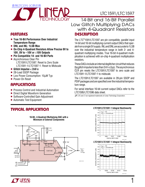
The LTC1591/LTC1597 series are high-precision 14-bit and 16-bit multiplying DACs featuring parallel input and current output capability. Designed for mission-critical systems, these units guarantee true 16-bit accuracy with remarkably low glitch impulses (<2nV-s) and include integrated 4-quadrant resistors. This manual provides comprehensive technical data, including electrical specifications, absolute maximum ratings, and application guidance necessary for integrating the converters into industrial automation, process control, and complex test equipment. Ideal for engineers requiring reliable, power-efficient, high-accuracy signal generation across wide temperature ranges.
📄 Preview PAGE OF 20

Page 1 Text Content

查询LTC1591-1C供应商

LTC1591/LTC1597

14-Bit and 16-Bit Parallel Low Glitch Multiplying DACs with 4-Quadrant Resistors FEATURES DESCRIPTION

True 16-Bit Performance Over Industrial The LTC®1591/LTC1597 are pin compatible, parallel input Temperature Range 14-bit and 16-bit multiplying current output DACs that oper- DNL and INL: 1LSB Max ate from a single 5V supply. INL and DNL are accurate to 1LSB On-Chip 4-Quadrant Resistors Allow Precise 0V to over the industrial temperature range in both 2- and 4- 10V, 0V to –10V or ±10V Outputs quadrant multiplying modes. True 16-bit 4-quadrant multi- Pin Compatible 14- and 16-Bit Parts plication is achieved with on-chip 4-quadrant multiplication Asynchronous Clear Pin resistors. LTC1591/LTC1597: Reset to Zero Scale

These DACs include an internal deglitcher circuit that reduces

LTC1591-1/LTC1597-1: Reset to Midscale

the glitch impulse to less than 2n V-s (typ). The asynchronous

Glitch Impulse < 2n V-s

CLR pin resets the LTC1591/LTC1597 to zero scale and

28-Lead SSOP Package

LTC1591-1/LTC1597-1 to midscale.

Low Power Consumption: 10µW Typ

The LTC1591/LTC1597 are available in 28-pin SSOP and

Power-On Reset

PDIP packages and are specified over the industrial tempera- APPLICATIONS ture range. For serial interface 16-bit current output DACs refer to the

Process Control and Industrial Automation

LTC1595/LTC1596 data sheet.

Direct Digital Waveform Generation IN TE GR AL ON LI NE AR IT (L SB IN TE GR AL ON LI NE AR IT (L SB , LTC and LT are registered trademarks of Linear Technology Corporation. Software-Controlled Gain Adjustment

Automatic Test Equipment

LTC1591/LTC1591-1 Integral Nonlinearity TYPICAL APPLICATION 1.0 VREF = 10V 0.8 VOUT = ±10V BIPOLAR 0.6

16-Bit, 4-Quadrant Multiplying DAC with a 0.4 Minimum of External Components 0.2

VREF –0.2

LT®1468

DIGITAL INPUT CODE

1591/97 TA02

R1 RCOM REF VCC ROFS RFB

15p F LTC1597/LTC1597-1 Integral Nonlinearity

R1 R2 RFBROFS

VREF = 10V 6IOUT1 0.8 VOUT = ±10V BIPOLAR

VOUT =

DATA LTC1597-1 LT146816-BIT DAC –VREF

AGND TO VREF 0.4

INPUTS

10 TO 21,

24 TO 27 DGND

WR LD CLR

1591/97 TA01

WR LD –0.6 CLR

DIGITAL INPUT CODE

1591/97 TA03

Page Summary Contents For LINEAR LTC1591 LTC1597 DATA SHEET

Page 1 查询LTC1591-1C供应商 LTC1591/LTC1597 14-Bit and 16-Bit Parallel Low Glitch Multiplying DACs with 4-Quadrant Resistors FEATURES DESCRIPTION True 16-Bit Performance Over Industrial The LTC®1591/LTC1597 are p...
Page 2 LTC1591/LTC1597 ABSOLUTE MAXIMUM RATINGS (Note 1) VCC to AGND 0.5V to 7V Operating Temperature Range VCC to DGND 0.5V to 7V LTC1591C/LTC1591-1C AGND to DGND VCC + 0.5V LTC1597C/LTC1597-1C 0°C to 70°C ...
Page 3 LTC1591/LTC1597 ELECTRICAL CHARACTERISTICS VCC = 5V ±10%, VREF = 10V, IOUT1 = AGND = DGND = 0V, TA = TMIN to TMAX, unless otherwise noted. LTC1591/-1 LTC1597B/-1B LTC1597A/-1A SYMBOL PARAMETER CONDITI...
Page 4 LTC1591/LTC1597 ELECTRICAL CHARACTERISTICS VCC = 5V ±10%, VREF = 10V, IOUT1 = AGND = DGND = 0V, TA = TMIN to TMAX, unless otherwise noted. SYMBOL PARAMETER CONDITIONS MIN TYP MAX UNITS Analog Outputs ...
Page 5 OU TP UT OL TA GE (m V) LTC1591/LTC1597 TYPICAL PERFOR A CE CHARACTERISTICS (LTC1591/LTC1597) SU PP LY UR RE NT (m A) SI GN AL /(N OI SE IS TO RT IO N) (d B) Unipolar Multiplying Mode Signal-to-(Noise...
Page 6 IN TE GR AL ON LI NE AR IT (L SB IN TE GR AL ON LI NE AR IT (L SB IN TE GR AL ON LI NE AR IT (L SB LTC1591/LTC1597 TYPICAL PERFOR A CE CHARACTERISTICS (LTC1591) Integral Nonlinearity vs Reference Volt...
Page 7 LTC1591/LTC1597 TYPICAL PERFOR A CE CHARACTERISTICS (LTC1591) AT TE NU AT IO (d B) DI FF ER EN TI AL ON LI NE AR IT (L SB Differential Nonlinearity vs Unipolar Multiplying Mode Frequency Supply Voltag...
Page 8 IN TE GR AL ON LI NE AR IT (L SB IN TE GR AL ON LI NE AR IT (L SB IN TE GR AL ON LI NE AR IT (L SB LTC1591/LTC1597 TYPICAL PERFOR A CE CHARACTERISTICS (LTC1597) Integral Nonlinearity vs Reference Volt...
Page 9 LTC1591/LTC1597 TYPICAL PERFOR A CE CHARACTERISTICS (LTC1597) AT TE NU AT IO (d B) DI FF ER EN TI AL ON LI NE AR IT (L SB Differential Nonlinearity vs Unipolar Multiplying Mode Frequency Supply Voltag...
Page 10 LTC1591/LTC1597 PIN FUNCTIONS LTC1591 IOUT1 (Pin 6): DAC Current Output. Tie to the inverting input of the current to voltage converter op amp. REF (Pin 1): Reference Input and 4-Quadrant Resistor R2....
Page 11 LTC1591/LTC1597 TRUTH TABLE Table 1 CONTROL INPUTS CLR WR LD REGISTER OPERATION Reset Input and DAC Register to All 0s for LTC1591/LTC1597 and Midscale for LTC1591-1/LTC1597-1 (Asynchronous Operation)...
Page 12 LTC1591/LTC1597 BLOCK DIAGRA SM LTC1597 REF RFB 48k 48k 48k 48k 48k 48k 48k 96k 96k 96k 96k 12k ROFS4 IOUT1 VCC AGND DECODER DGND22 (MSB) (LSB)LOAD LD RST CLR28 DAC REGISTER WR WR INPUT REGISTER RST 1...
Page 13 LTC1591/LTC1597 APPLICATIONS INFORMATION Description Digital Section The LTC1591/LTC1597 are 14-/16-bit multiplying, current The LTC1591/LTC1597 are 14-/16-bit wide full parallel output DACs with a fu...
Page 14 LTC1591/LTC1597 APPLICATIONS INFORMATION R1 RCOM REF VCC ROFS RFB Unipolar Binary Code Table R1 R2 RFBROFS 6IOUT1 DIGITAL INPUT VOUT = BINARY NUMBER ANALOG OUTPUT DATA LTC1597 LT1001 16-BIT DAC 0V TO ...
Page 15 LTC1591/LTC1597 APPLICATIONS INFORMATION VREF 1/2 LT1112 R1 RCOM REF VCC ROFS RFB 33p F Bipolar Offset Binary Code Table R1 RFBROFS DIGITAL INPUT 6IOUT1 BINARY NUMBER ANALOG OUTPUT VOUT = IN DAC REGIS...
Page 16 LTC1591/LTC1597 TYPICAL APPLICATIONS Noninverting Unipolar Operation (2-Quadrant Multiplication) VOUT = 0V to VREF 1/2 LT1112 RCOM REF VCC ROFS RFB R1 RFBROFS 6IOUT1 VOUT = DATA LTC1597 1/2 LT111216-B...
Page 17 LTC1591/LTC1597 TYPICAL APPLICATIONS 16-Bit VOUT DAC Programmable Unipolar/Bipolar Configuration LTC203AC UNIPOLAR/ BIPOLAR LT1468 LT1236A-10 LT1001 R1 RCOM REF VCC ROFS RFB R1 RFBROFS 6IOUT1 DATA LTC...
Page 18 LTC1591/LTC1597 TYPICAL APPLICATIONS Digital Waveform Generator LT1236A-10 LT1001 PHASE ACCUMULATOR R1 RCOM REF VCC ROFS RFB FREQUENCY CONTROL R1 R2 RFBROFS 6IOUT1 PARALLEL DELTA nnn SERIAL SIN ROM OR...
Page 19 LTC1591/LTC1597 PACKAGE DESCRIPTION Dimensions in inches (millimeters) unless otherwise noted. G Package 28-Lead Plastic SSOP (0.209) (LTC DWG # 05-08-1640) BSC 0.002 – 0.008 0.010 – 0.015 (0.25 – 0.3...
Page 20 LTC1591/LTC1597 TYPICAL APPLICATION 17-Bit Sign Magnitude DAC with Bipolar Zero Error of 140µV (0.92LSB at 17 Bits) at 25°C LTC203AC LT1236A-10 LT1468 R1 RCOM REF VCC ROFS RFB R1 RFBROFS 6IOUT1 DATA L...

Manual Details

Brand Linear
Pages 20
File Size 370.26 KB
Published June 20, 2026
1 views

Enter the captcha to get the download link:

captcha

Frequently Asked Questions

What are the DAC conversion bit depths available?

The devices offer interchangeable 14-bit and 16-bit performance parts that utilize parallel input technology.

How is glitch energy handled by these DACs?

They include an internal deglitcher circuit designed to reduce the glitch impulse to less than $2 ext{nV-s}$ (typ).

What are the methods for resetting the device scale?

The asynchronous CLR pin can reset the chip to zero scale, and Power-On Reset (POR) resets it to midscale.

What kind of output signal do these parts provide?

They are multiplying current output DACs that allow for 4-quadrant multiplication in unipolar or bipolar modes.