LINEAR LTC1345 Data Sheet
Summary
The LTC1345 is a robust single-chip V.35 transceiver delivering both clock and data signals for reliable communication interfaces. Designed to operate entirely from a single 5V supply, it features three independent transmitters and receivers with built-in ESD and short-circuit protection. This manual provides comprehensive technical specifications, electrical characteristics, operating ranges, and application details necessary for integrating the component into complex electronic systems. It is essential documentation for hardware engineers and industrial designers building equipment that requires standardized V.35 connectivity ports (DTE or DCE).
Page 1 Text Content
查询LTC1345CNW供应商
LTC1345 Single Supply V.35 Transceiver
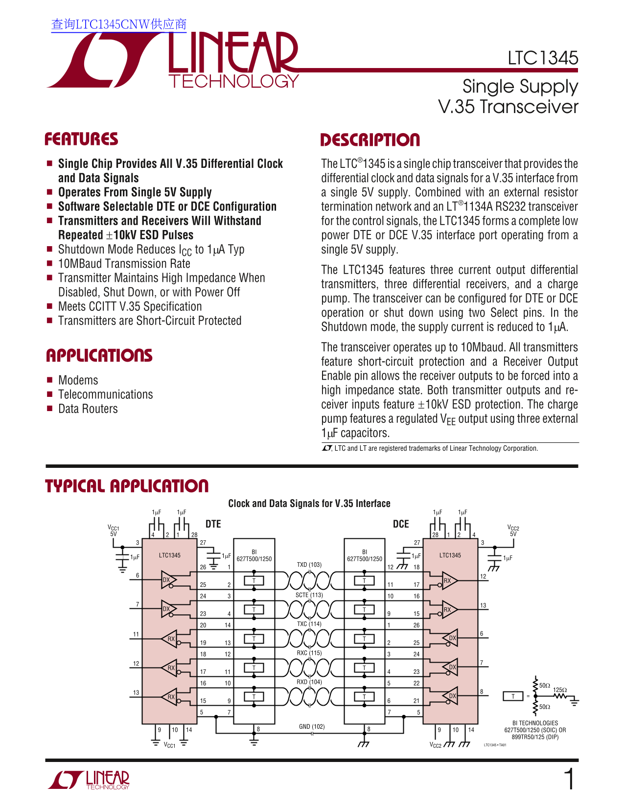
FEATURES DESCRIPTIO Single Chip Provides All V.35 Differential Clock The LTC®1345 is a single chip transceiver that provides the and Data Signals differential clock and data signals for a V.35 interface from Operates From Single 5V Supply a single 5V supply. Combined with an external resistor Software Selectable DTE or DCE Configuration termination network and an LT®1134A RS232 transceiver Transmitters and Receivers Will Withstand for the control signals, the LTC1345 forms a complete low Repeated ±10k V ESD Pulses power DTE or DCE V.35 interface port operating from a Shutdown Mode Reduces ICC to 1µA Typ single 5V supply. 10MBaud Transmission Rate
The LTC1345 features three current output differential
Transmitter Maintains High Impedance When
transmitters, three differential receivers, and a charge
Disabled, Shut Down, or with Power Off
pump. The transceiver can be configured for DTE or DCE
Meets CCITT V.35 Specification
operation or shut down using two Select pins. In the
Transmitters are Short-Circuit Protected
Shutdown mode, the supply current is reduced to 1µA. The transceiver operates up to 10Mbaud. All transmitters
APPLICATIO S
feature short-circuit protection and a Receiver Output Enable pin allows the receiver outputs to be forced into a
Modems
high impedance state. Both transmitter outputs and re-
Telecommunications
ceiver inputs feature ±10k V ESD protection. The charge
Data Routers
pump features a regulated VEE output using three external 1µF capacitors. , LTC and LT are registered trademarks of Linear Technology Corporation.
TYPICAL APPLICATIO
Clock and Data Signals for V.35 Interface
VCC1 DCEDTE VCC2
1µF LTC1345 1µF 1µF LTC1345BI
TXD (103)
DX RXT
SCTE (113)
DX RXT
TXC (114)
RX DX
RXC (115)
RX DX
RXD (104)
RX DX
BI TECHNOLOGIES
GND (102)
627T500/1250 (SOIC) OR 899TR50/125 (DIP)
VCC1 VCC2 LTC1345 • TA01
Page Summary Contents For LINEAR LTC1345 Data Sheet
Manual Details
| Brand | Linear |
|---|---|
| Pages | 12 |
| File Size | 206.39 KB |
| Published | July 15, 2026 |
Enter the captcha to get the download link:

Frequently Asked Questions
How can I configure the LTC1345 as DTE or DCE?
The transceiver features two Select pins that allow it to be configured for either DTE or DCE mode. Uyghur
What is the maximum transmission data rate supported by this chip?
The LTC1345 operates up to 10 Mbaud.
Are there safeguards against electrical damage like surges?
Yes, all transmitter and receiver inputs feature –10kV ESD protection, and transmitters are short-circuit protected.