# A B C D E F G H I J K L M N O P Q R S T U V W X Y Z

LINEAR LT6202, LT6203, LT6204 Data Sheet

Summary

Experience superior signal integrity with this series of ultralow noise operational amplifiers. These high-performance, low-power Op Amps feature 1.9nV/√Hz noise voltage, a massive 100MHz bandwidth, and reliable rail-to-rail operation across a wide supply range (2.5V–12.6V). The comprehensive manual details electrical specifications, multiple package options (including tiny DFN), and diverse applications, making it essential for engineers designing compact, battery-powered signal conditioning systems and advanced data acquisition circuitry.
📄 Preview PAGE OF 24

Page 1 Text Content

查询LT6202CS5供应商

LT6202/LT6203/LT6204 Single/Dual/Quad 100MHz,

Rail-to-Rail Input and Output,

Ultralow 1.9n V/√Hz Noise, Low Power Op Amps

FEATURES DESCRIPTIO

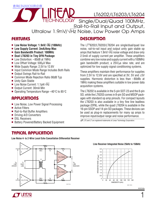
Low Noise Voltage: 1.9n V/√Hz (100k Hz) The LT®6202/LT6203/LT6204 are single/dual/quad low Low Supply Current: 3m A/Amp Max noise, rail-to-rail input and output unity gain stable op Gain Bandwidth Product: 100MHz amps that feature 1.9n V/√Hz noise voltage and draw only Dual LT6203 in Tiny DFN Package 2.5m A of supply current per amplifier. These amplifiers

Low Distortion: –80d B at 1MHz combine very low noise and supply current with a 100MHz Low Offset Voltage: 500µV Max gain bandwidth product, a 25V/µs slew rate, and are Wide Supply Range: 2.5V to 12.6V optimized for low supply signal conditioning systems.

Input Common Mode Range Includes Both Rails

These amplifiers maintain their performance for supplies

Output Swings Rail-to-Rail

from 2.5V to 12.6V and are specified at 3V, 5V and ±5V

Common Mode Rejection Ratio 90d B Typ

supplies. Harmonic distortion is less than –80d Bc at

Unity Gain Stable

1MHz making these amplifiers suitable in low power data

Low Noise Current: 1.1p A/√Hz

acquisition systems.

Output Current: 30m A Min

Operating Temperature Range –40°C to 85°C The LT6202 is available in the 5-pin SOT-23 and the 8-pin SO, while the LT6203 comes in 8-pin SO and MSOP pack-

IN TE GR AT ED OI SE (µ S)

APPLICATIO ages with standard op amp pinouts. For compact layouts the LT6203 is also available in a tiny fine line leadless

Low Noise, Low Power Signal Processing

package (DFN), while the quad LT6204 is available in the

Active Filters

16-pin SSOP and 14-pin SO packages. These devices can

Rail-to-Rail Buffer Amplifiers

be used as plug-in replacements for many op amps to

Driving A/D Converters

improve input/output range and noise performance.

DSL Receivers

, LTC and LT are registered trademarks of Linear Technology Corporation.

Battery Powered/Battery Backed Equipment

TYPICAL APPLICATIO Low Noise 4- to 2-Wire Local Echo Cancellation Differential Receiver

Line Receiver Integrated Noise 25k Hz to 150k Hz

1/2 LT1739 5.0

1/2 LT6203

VD ••VL VR

LINE 100Ω LINE 2.5

DRIVER LINE RECEIVER

1/2 LT6203

1/2 LT1739

BANDWIDTH (k Hz)

6203 TA01a

6203 • TA01b

620234fa

Page Summary Contents For LINEAR LT6202, LT6203, LT6204 Data Sheet

Page 1 查询LT6202CS5供应商 LT6202/LT6203/LT6204 Single/Dual/Quad 100MHz, Rail-to-Rail Input and Output, Ultralow 1.9n V/√Hz Noise, Low Power Op Amps FEATURES DESCRIPTIO Low Noise Voltage: 1.9n V/√Hz (100k Hz) The...
Page 2 LT6202/LT6203/LT6204 ABSOLUTE AXI RATI GS (Note 1) Total Supply Voltage (V+ to V–) 12.6V Junction Temperature (DD Package) 125°C Input Current (Note 2) ±40m A Storage Temperature Range ..................
Page 3 LT6202/LT6203/LT6204 PACKAGE/ORDER I FOR ATIO TOP VIEW ORDER PART ORDER PART TOP VIEW OUT A OUT D NUMBER NUMBER OUT A OUT D –IN A –IN D LT6204CGN –IN A –IN D LT6204CS +IN A +IN D LT6204IGN +IN A +IN D...
Page 4 LT6202/LT6203/LT6204 ELECTRICAL CHARACTERISTICS TA = 25°C, VS =5V, 0V; VS = 3V, 0V; VCM = VOUT = half supply, unless otherwise noted. SYMBOL PARAMETER CONDITIONS MIN TYP MAX UNITS CIN Input Capacitanc...
Page 5 LT6202/LT6203/LT6204 ELECTRICAL CHARACTERISTICS The ● denotes the specifications which apply over 0°C < TA < 70°C temperature range. VS = 5V, 0V; VS = 3V, 0V; VCM = VOUT = half supply, unless ot...
Page 6 LT6202/LT6203/LT6204 ELECTRICAL CHARACTERISTICS The ● denotes the specifications which apply over –40°C < TA < 85°C temperature range. VS = 5V, 0V; VS = 3V, 0V; VCM = VOUT = half supply, unless ...
Page 7 LT6202/LT6203/LT6204 TA = 25°C, VS = ±5V; VCM = VOUT = 0V, unless otherwise noted.ELECTRICAL CHARACTERISTICS SYMBOL PARAMETER CONDITIONS MIN TYP MAX UNITS VOS Input Offset Voltage LT6203, LT6204, LT62...
Page 8 LT6202/LT6203/LT6204 ELECTRICAL CHARACTERISTICS The ● denotes the specifications which apply over 0°C < TA < 70°C temperature range. VS = ±5V; VCM = VOUT = 0V, unless otherwise noted. SYMBOL PAR...
Page 9 LT6202/LT6203/LT6204 ELECTRICAL CHARACTERISTICS The ● denotes the specifications which apply over –40°C < TA < 85°C temperature range. VS = ±5V; VCM = VOUT = 0V, unless otherwise noted. (Note 5)...
Page 10 IN PU BI AS UR RE NT (µ A) SU PP LY UR RE NT (m A) NU BE OF NI TS LT6202/LT6203/LT6204 TYPICAL PERFOR A CE CHARACTERISTICS VOS Distribution, VCM = V+/2 VOS Distribution, VCM = V+ VOS Distribution, VCM...
Page 11 CH AN GE IN FF SE VO LT AG (µ V) IN PU VO LT AG (m V) CH AN GE IN FF SE VO LT AG (m V) LT6202/LT6203/LT6204 TYPICAL PERFOR A CE CHARACTERISTICS Output Short-Circuit Current vs Minimum Supply Voltage P...
Page 12 PHASE (DEG) GA IN AN DW IT (M Hz IN AN DW IT (M Hz BA LA NC ED OI SE UR RE NT (p A/ √H z) LT6202/LT6203/LT6204 TYPICAL PERFOR A CE CHARACTERISTICS Balanced Noise Current vs Unbalanced Noise Current vs...
Page 13 SE TT LI NG IM (n s) OV ER SH OO CO ON OD RE JE CT IO RA TI (d B) LT6202/LT6203/LT6204 TYPICAL PERFOR A CE CHARACTERISTICS Common Mode Rejection Ratio Power Supply Rejection Ratio vs Frequency Channel...
Page 14 DI ST OR TI ON (d Bc LT6202/LT6203/LT6204 TYPICAL PERFOR A CE CHARACTERISTICS 2V /D IV 1V /D IV Distortion vs Frequency Distortion vs Frequency Distortion vs Frequency –40 –30 –40 AV = 1 AV = 2 AV = 2...
Page 15 LT6202/LT6203/LT6204 APPLICATIO S I FOR ATIO Amplifier Characteristics Input bias current normally flows out of the + and – inputs. The magnitude of this current increases when the input Figure 1 show...
Page 16 LT6202/LT6203/LT6204 APPLICATIO S I FOR ATIO Input Protection a diode drop of the input signal. In this photo, the input signal generator is clipping at ±35m A, and the output There are back-to-back d...
Page 17 LT6202/LT6203/LT6204 TYPICAL APPLICATIO Low Noise, Low Power 1MΩ AC output therefore sit at a point slightly higher than one Photodiode Transimpedance Amplifier pinchoff voltage below ground (typicall...
Page 18 LT6202/LT6203/LT6204 TYPICAL APPLICATIO Single-Supply 16-Bit ADC Driver Although the LTC1864 has a sample rate far below the gain bandwidth of the LT6203, using this amplifier is not Figure 5 shows th...
Page 19 LT6202/LT6203/LT6204 PACKAGE DESCRIPTIO DD Package 8-Lead Plastic DFN (3mm × 3mm) (Reference LTC DWG # 05-08-1698) (2 SIDES)2.15 ±0.05 (4 SIDES) (2 SIDES) PIN 1 TOP MARK PACKAGE OUTLINE (DD8) DFN 0203...
Page 20 LT6202/LT6203/LT6204 PACKAGE DESCRIPTIO MS8 Package 8-Lead Plastic MSOP (Reference LTC DWG # 05-08-1660) 0.42 ± 0.04 0.65 (.118 ± .004) 0.52 (.0165 ± .0015) (.0256) (NOTE 3) (.206) TYP BSC REF RECOMME...
Page 21 LT6202/LT6203/LT6204 PACKAGE DESCRIPTIO S8 Package 8-Lead Plastic Small Outline (Narrow .150 Inch) (Reference LTC DWG # 05-08-1610) NOTE 3 .050 BSC MIN .150 – .157 NOTE 3 .030 ±.005 TYP RECOMMENDED SO...
Page 22 LT6202/LT6203/LT6204 PACKAGE DESCRIPTIO S Package 14-Lead Plastic Small Outline (Narrow .150 Inch) (Reference LTC DWG # 05-08-1610) .050 BSC NOTE 3 .228 – .244 .150 – .157 (5.791 – 6.197) (3.810 – 3.9...
Page 23 LT6202/LT6203/LT6204 PACKAGE DESCRIPTIO S5 Package 5-Lead Plastic TSOT-23 (Reference LTC DWG # 05-08-1635) 2.90 BSC MAX REF (NOTE 4) 1.22 REF 3.85 MAX 1.4 MIN2.62 REF (NOTE 4)2.80 BSC PIN ONE RECOMMEN...
Page 24 LT6202/LT6203/LT6204 TYPICAL APPLICATIO Low Noise Differential Amplifier with Gain Adjust and Common Mode Control VIN 6d B 1/2 LT6203 RE LA TI VE IF FE RE NT IA GA IN (1 d B /D IV 0d B 1/2 LT6203 VOUT...

Manual Details

Brand Linear
Pages 24
File Size 574.59 KB
Published June 18, 2026
1 views

Enter the captcha to get the download link:

captcha

Frequently Asked Questions

What is the specified operating temperature range for these amplifiers?

The specified operating temperature range is –40°C to 85°C.

Are these op amps rail-to-rail and low noise?

Yes, they feature 1.9nV/√Hz noise voltage and maintain rail-to-rail output swinging from 2.5V to 12.6V.

What is the maximum gain bandwidth product (GBP)?

The amplifiers have a high gain bandwidth product of 100MHz.

How much power do these devices consume?

They draw very low supply current, for example, the LT6203 draws only 2.5mA per amplifier in the Tiny DFN package.