LINEAR LT3710 User Guide
Summary
The LT3710 is a high-efficiency step-down switching DC/DC converter regulator engineered to provide regulated, isolated auxiliary outputs for complex power supplies. Featuring dual synchronous N-channel MOSFET drivers and support for multiple output voltages (e.g., 3.3V and 1.8V) in a compact package, this regulator excels in offline and secondary side applications requiring high reliability up to 500kHz. This manual provides comprehensive technical specifications, detailed electrical parameters, application guidance, and recommended PCB layouts for engineers designing advanced isolated DC/DC converter topologies.
Page 1 Text Content
查询3710EFE供应商
LT3710
Secondary Side
Synchronous Post Regulator
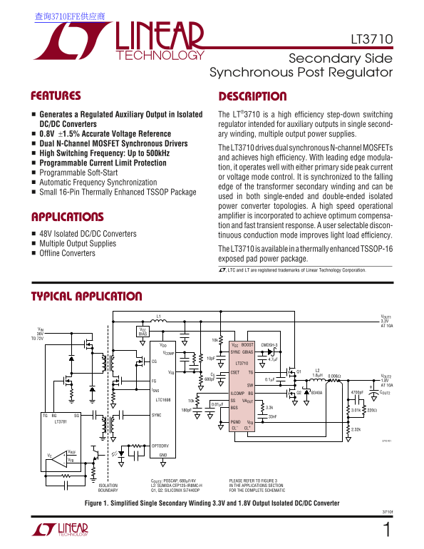
FEATURES DESCRIPTIO Generates a Regulated Auxiliary Output in Isolated The LT®3710 is a high efficiency step-down switching DC/DC Converters regulator intended for auxiliary outputs in single second- 0.8V ±1.5% Accurate Voltage Reference ary winding, multiple output power supplies. Dual N-Channel MOSFET Synchronous Drivers
The LT3710 drives dual synchronous N-channel MOSFETs
High Switching Frequency: Up to 500k Hz
and achieves high efficiency. With leading edge modula-
Programmable Current Limit Protection
tion, it operates well with either primary side peak current
Programmable Soft-Start
or voltage mode control. It is synchronized to the falling
Automatic Frequency Synchronization
edge of the transformer secondary winding and can be
Small 16-Pin Thermally Enhanced TSSOP Package
used in both single-ended and double-ended isolated power converter topologies. A high speed operational APPLICATIO S amplifier is incorporated to achieve optimum compensa- tion and fast transient response. A user selectable discon-
48V Isolated DC/DC Converters tinuous conduction mode improves light load efficiency. Multiple Output Supplies
The LT3710 is available in a thermally enhanced TSSOP-16
Offline Converters
exposed pad power package. , LTC and LT are registered trademarks of Linear Technology Corporation.
TYPICAL APPLICATIO
L1 VOUT1 3.3V AT 10A
VIN VCC 36V BIAS TO 72V
VDD VCC BOOST CMDSH-3 VCOMP SYNC GBIAS
LT3710
VFB TGCSET
CS 1.8µH VOUT2
SW AT 10A
Q2 B340A 4700p F COUT2
ILCOMP BG
LTC1698 10k SS VAOUT
BGS 3.3k
TG BG SG SYNC
LT3781 PGND VFB
CL– CL+ 2.32k
OPTODRV
VC GND
COUT2: POSCAP, 680µF/4V PLEASE REFER TO FIGURE 3
ISOLATION L2: SUMIDA CEP125-IR8MC-H IN THE APPLICATIONS SECTION BOUNDARY Q1, Q2: SILICONIX Si7440DP FOR THE COMPLETE SCHEMATIC
Figure 1. Simplified Single Secondary Winding 3.3V and 1.8V Output Isolated DC/DC Converter
Page Summary Contents For LINEAR LT3710 User Guide
Manual Details
| Brand | Linear |
|---|---|
| Pages | 12 |
| File Size | 208.16 KB |
| Published | June 18, 2026 |
Enter the captcha to get the download link:

Frequently Asked Questions
What is the maximum switching frequency?
The LT3710 can operate at a high switching frequency, up to 500kHz.
How does the device achieve stable operation and fast transient response?
It incorporates a high-speed operational amplifier for optimum compensation and fast transient response.
What is the safe operating junction temperature range?
The required operating junction temperature range is -40°C to 125°C.
Is specific PCB layout needed when using the exposed pad?
The exposed pad(s) must be connected to PGND and soldered to the PCB.