LINEAR LT3582 User Guide
Summary
Streamline power delivery with this advanced dual switching regulator, designed to generate multiple positive and negative voltage outputs from a single supply source. The unit is highly integrated into a compact footprint, ensuring maximum efficiency and minimum ripple for demanding applications like AMOLED displays, CCD cameras, and complex op-amp circuits. This resource provides comprehensive details on system design, including power-up sequencing, programmable current adjustment, and high-efficiency operation across varying load ranges, making it essential for embedded electronics designers tackling multi-voltage systems.
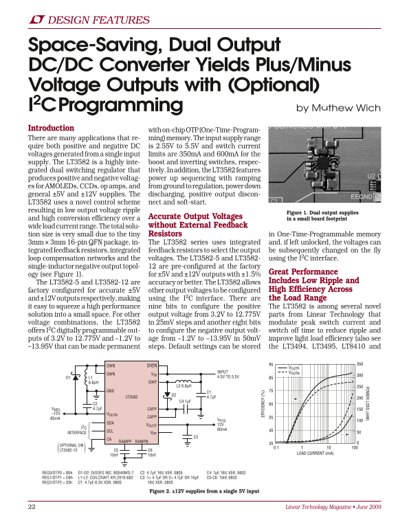
Page 1 Text Content
L DESIGN FEATURES
POW ER LOSS (m
Space-Saving, Dual Output DC/DC Converter Yields Plus/Minus Voltage Outputs with (Optional) I2C Programming by Mathew Wich Introduction with on-chip OTP (One-Time-Program- There are many applications that re- ming) memory. The input supply range quire both positive and negative DC is 2.55V to 5.5V and switch current voltages generated from a single input limits are 350m A and 600m A for the supply. The LT3582 is a highly inte- boost and inverting switches, respec- grated dual switching regulator that tively. In addition, the LT3582 features produces positive and negative voltag- power up sequencing with ramping es for AMOLEDs, CCDs, op amps, and from ground to regulation, power down general ±5V and ±12V supplies. The discharging, positive output discon- LT3582 uses a novel control scheme nect and soft-start. resulting in low output voltage ripple
Figure 1. Dual output supplies
and high conversion efficiency over a Accurate Output Voltages
in a small board footprint
wide load current range. The total solu- without External Feedback
tion size is very small due to the tiny Resistors in One-Time-Programmable memory 3mm × 3mm 16-pin QFN package, in- The LT3582 series uses integrated and, if left unlocked, the voltages can tegrated feedback resistors, integrated feedback resistors to select the output be subsequently changed on the fly loop compensation networks and the voltages. The LT3582-5 and LT3582- using the I2C interface.
EF FI CI EN CY
single-inductor negative output topol- 12 are pre-configured at the factory
Great Performance
ogy (see Figure 1). for ±5V and ±12V outputs with ±1.5%
The LT3582-5 and LT3582-12 are accuracy or better. The LT3582 allows Includes Low Ripple and factory configured for accurate ±5V other output voltages to be configured High Efficiency Across
and ±12V outputs respectively, making using the I2C interface. There are the Load Range it easy to squeeze a high performance nine bits to configure the positive The LT3582 is among several novel solution into a small space. For other output voltage from 3.2V to 12.775V parts from Linear Technology that voltage combinations, the LT3582 in 25m V steps and another eight bits modulate peak switch current and offers I2C digitally programmable out- to configure the negative output volt- switch off time to reduce ripple and puts of 3.2V to 12.775V and –1.2V to age from –1.2V to –13.95V in 50m V improve light load efficiency (also see –13.95V that can be made permanent steps. Default settings can be stored the LT3494, LT3495, LT8410 and
SWN SHDN
VOUTP
INPUT VOUTN
SWN VIN
D1 L1 4.5V TO 5.5V
6.8µH SWP
GND C1
LT3582 4.7µF
C2 VNEG 4.7µF CAPP
–12V VOUTN
VOUTP 12V
INTERFACE VPP
RAMPNRAMPP
OPTIONAL ON
LT3582-12 C5 C6
LOAD CURRENT (m A)
REG0/OTP0 = B0h D1-D2: DIODES INC. B0540WS-7 C2: 4.7µF, 16V, X5R, 0805 C4: 1µF, 16V, X5R, 0603 REG1/OTP1 = D8h L1-L2: COILCRAFT XPL2010-682 C3: 1 4.7µF OR 2 4.7µF OR 10µF C5-C6: 10n F, 0603
REG2/OTP2 = 03h C1: 4.7µF, 6.3V, X5R, 0805 16V, X5R, 0805
Figure 2. ±12V supplies from a single 5V input
Linear Technology Magazine • June 2009
Page Summary Contents For LINEAR LT3582 User Guide
Manual Details
| Brand | Linear |
|---|---|
| Pages | 4 |
| File Size | 844.93 KB |
| Published | June 16, 2026 |
Enter the captcha to get the download link:

Frequently Asked Questions
What voltage supplies does the LT3582 support?
It handles positive and negative voltages, with examples including ±5V and ±12V.
Can the output voltages be adjusted digitally?
Yes, it features a digitally programmable interface using an IC to set various output voltages from 3.2V to 12.775V and –1.2V to –13.95V in fine steps.
How does the LT3582 improve efficiency at low loads?
It uses a novel control scheme that reduces load current dramatically, improving light load efficiency and moderating output ripple.
What is the primary function of the LTC4217?
The primary role is to act as an electronic circuit breaker for protection of the MOSFET, with features like overcurrent timeout and thermal protection.