LINEAR dn412f Data Sheet
Summary
The LT3681 is an advanced, highly integrated 36V buck regulator designed for power-constrained applications. It simplifies complex converter design by combining the power switch and Schottky diode into a single, small package, dramatically reducing board footprint. This manual provides a comprehensive look at its performance, covering wide input voltage support (3.6V to 34V), adjustable frequency, and high efficiency across variable loads. Perfect for professional designers building robust, space-saving power supplies that require extremely low output ripple and maximum battery life.
Page 1 Text Content
36V 2A Buck Regulator Integrates Power Schottky Design Note 412 David Ng
Introduction A Small, Simple Solution Everyone wants more power in less space. However, the The LT3681 integrates a wide input voltage range, high task of designing a power supply is easy to describe but performance buck controller, power switch, high side diffi cult to execute. How does a designer select an optimal bootstrapping boost diode and a power Schottky diode. All set of components that yields the best possible power of these attributes are crammed into a tiny but thermally supply in terms of size, cost and performance? Well, it effi cient 14-pin 3mm × 4mm DFN package. So, all a de- is easier if the selection is reduced to only a handful of signer needs to implement a full-featured buck converter components. is to add the output LC fi lter and a few passives. For instance, the LT®3681 reduces parts selection to only The most obvious advantage of having the power Schottky a few passive components by integrating all of the power diode integrated into the LT3681 is space savings, reduc-
EF FI CI EN CY
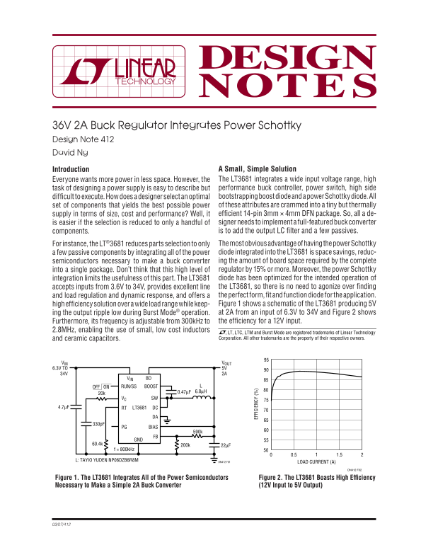
semiconductors necessary to make a buck converter ing the amount of board space required by the complete into a single package. Don’t think that this high level of regulator by 15% or more. Moreover, the power Schottky integration limits the usefulness of this part. The LT3681 diode has been optimized for the intended operation of accepts inputs from 3.6V to 34V, provides excellent line the LT3681, so there is no need to agonize over fi nding and load regulation and dynamic response, and offers a the perfect form, fi t and function diode for the application. high effi ciency solution over a wide load range while keep- Figure 1 shows a schematic of the LT3681 producing 5V ing the output ripple low during Burst Mode® operation. at 2A from an input of 6.3V to 34V and Figure 2 shows Furthermore, its frequency is adjustable from 300k Hz to the effi ciency for a 12V input.
2.8MHz, enabling the use of small, low cost inductors
, LT, LTC, LTM and Burst Mode are registered trademarks of Linear Technology and ceramic capacitors. Corporation. All other trademarks are the property of their respective owners.
VIN VOUT 6.3V TO 5V 34V 2A
VIN BD
OFF ON RUN/SS BOOST
VC SW
4.7µF RT LT3681 DC
PG BIAS
FB GND
f = 800k Hz
L: TAYIO YUDEN NP06DZB6R8M DN412 F01
LOAD CURRENT (A)
Figure 1. The LT3681 Integrates All of the Power Semiconductors Figure 2. The LT3681 Boasts High Effi ciency Necessary to Make a Simple 2A Buck Converter (12V Input to 5V Output)
Page Summary Contents For LINEAR dn412f Data Sheet
Manual Details
| Brand | Linear |
|---|---|
| Pages | 2 |
| File Size | 81.54 KB |
| Published | June 15, 2026 |
Enter the captcha to get the download link:

Frequently Asked Questions
What is the input voltage range of the LT3681?
The LT3681 accepts inputs from 3.6V to 34V.
How much board space does the LT3681 save?
It reduces the required board space for the complete regulator by 15% or more.
What is the no load output voltage ripple in Burst Mode?
The no load output voltage ripple is kept below 15mV P-P during Burst Mode operation.