LINEAR dn1013f Data Sheet
Summary
Master critical techniques for understanding clock jitter's impact on high-speed Analog-to-Digital Converters (ADCs). This manual offers detailed electrical insights into aperture uncertainty and how timing errors degrade Signal-to-Noise Ratio (SNR) performance at demanding signal rates. Essential reading for RF, DSP, or instrumentation engineers designing data acquisition systems that require ultra-low jitter clock sources.
Page 1 Text Content
advertisement
Understanding the Effect of Clock Jitter on High Speed ADCs Design Note 1013 Derek Redmayne (LTC Applications Engineer), Eric Trelewicz (LTC Applications Manager) and Alison Smith (High Speed ADC Product Marketing Engineer)
Digitizing high speed signals to a high resolution requires tone, or a narrow band, with equivalent power at 1MHz. careful selection of a clock that will not compromise the
There are various contributors to jitter in any scenario,
sampling performance of the Analog to Digital Converter
extending from the oscillator to any frequency dividers,
(ADC). In this article we hope to give the reader a bet-
clock buffers and any noise acquired due to coupling
ter understanding of clock jitter and how it affects the
effects, in addition to the internal aperture jitter of the
performance of the high speed ADC.
ADC itself.
As an example we will highlight the latest high perfor-
The internal aperture jitter of the LTC2209 is 70fempto
mance ADC from Linear Technology, the 16-bit, 160Msps
seconds. For the level of performance exhibited by the
LTC2209. This ADC exhibits a signal to noise ratio (SNR)
LTC2209 and other members in Linear Technology’s high
of 77.4d B, with 100d B SFDR throughout much of the
speed 16-bit family, 0.5ps, the best available from many
baseband region. Like most high speed ADCs on the
oscillator vendors, may produce discernable compromise
market today, the LTC2209 uses a sample-and-hold (S&H)
in SNR for some sampling scenarios. It is not the ADC
circuit that essentially takes a snapshot of the ADC input
but the sampling scenario that dictates the required jitter
at an instant in time. When the S&H switch is closed,
performance. Any ADC that exhibits 77d B SNR at 140MHz
the network at the input of the ADC is connected to the
input frequency would require the same jitter performance
sample capacitor. At the instant the switch is opened
to achieve full data sheet SNR. It is the input frequency
one half clock cycle later, the voltage on the capacitor
not the clock frequency that is the determining factor with
is recorded and held. Variation in the time at which the
respect to jitter performance. On the LTC2209 a clock
switch is opened is known as aperture uncertainty, or jit-
that has 10ps jitter would only cause a loss of about
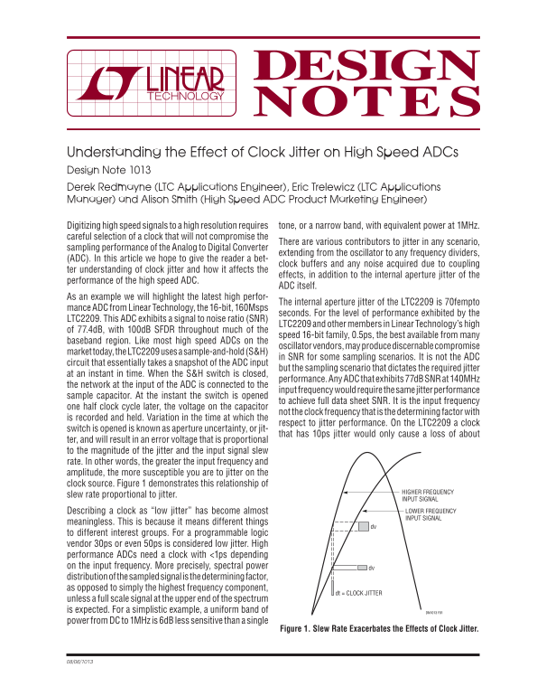
ter, and will result in an error voltage that is proportional to the magnitude of the jitter and the input signal slew rate. In other words, the greater the input frequency and amplitude, the more susceptible you are to jitter on the clock source. Figure 1 demonstrates this relationship of
HIGHER FREQUENCY
slew rate proportional to jitter.
INPUT SIGNAL Describing a clock as “low jitter” has become almost LOWER FREQUENCY INPUT SIGNAL
meaningless. This is because it means different things
to different interest groups. For a programmable logic vendor 30ps or even 50ps is considered low jitter. High performance ADCs need a clock with <1ps depending on the input frequency. More precisely, spectral power dv distribution of the sampled signal is the determining factor, as opposed to simply the highest frequency component,
dt = CLOCK JITTER
unless a full scale signal at the upper end of the spectrum is expected. For a simplistic example, a uniform band of DN1013 F01 power from DC to 1MHz is 6d B less sensitive than a single
Figure 1. Slew Rate Exacerbates the Effects of Clock Jitter.
Page Summary Contents For LINEAR dn1013f Data Sheet
Manual Details
| Brand | Linear |
|---|---|
| Pages | 4 |
| File Size | 112.30 KB |
| Published | June 16, 2026 |
Enter the captcha to get the download link:

Frequently Asked Questions
How does clock jitter affect the ADC's performance?
Jitter degrades the Signal-to-Noise Ratio (SNR). Higher input frequencies and amplitude make the system more susceptible to jitter.
What is required for a high-speed ADCs regarding clock quality?
A clock with less than 1ps of jitter is needed, depending on the input frequency. Spectral power distribution is key, not just the highest frequency component.
What causes compromise in ADC clocks besides the oscillator?
Poor PCB routing (like sharing conduits for digital signals) and excessive ground bounce can compromise the clock signal.
Is it safe to use a DLL to generate low-frequency clocks?
No, do not use a Delay Locked Loop (DLL) to produce a clock as low as 20kHz, unless you are over-sampling the audio band.