LINEAR Design Note DN473: Using a Differential I/O Amplifier in Single-Ended Applications
Summary
Optimize your analog circuits using fully differential I/O amplifiers for reliable single-ended signal processing. This design note provides expert analysis detailing how to adapt specialized op amps—like the LTC6406—for optimal performance in simplified, low-voltage applications. It is essential reading for electrical engineers and hardware designers seeking stable, high-precision solutions while minimizing common mode noise and maximizing signal swing efficiency.
Page 1 Text Content
Using a Differential I/O Amplifi er in Single-Ended Applications Design Note DN473 Glen Brisebois Introduction the voltage applied at VOCM. One fi nal observation is that
Recent advances in low voltage silicon germanium there is no longer a single inverting input: both inputs are and Bi CMOS processes have allowed the design and inverting and noninverting depending on which output production of very high speed amplifi ers. Because the is considered. For the purposes of circuit analysis, the processes are low voltage, most of the amplifi er designs inputs are labeled with “+” and “–” in the conventional have incorporated differential inputs and outputs to regain manner and one output receives a dot, denoting it as the and maximize total output signal swing. Since many low- inverted output for the “+” input.
voltage applications are single-ended, the questions arise,
Anybody familiar with conventional op amps knows that
“How can I use a differential I/O amplifi er in a single-ended
noninverting applications have inherently high input
application?” and “What are the implications of such
impedance at the noninverting input, approaching GΩ or
use?” This Design Note addresses some of the practical
even TΩ. But in the case of the fully differential op amp
implications and demonstrates specifi c single-ended
in Figure 1, there is feedback to both inputs, so there is
applications using the 3GHz gain-bandwidth LTC6406
no high impedance node. Fortunately this diffi culty can
differential I/O amplifi er.
be overcome.
Background
RI2 RF2
A conventional op amp has two differential inputs and an output. The gain is nominally infi nite, but control
is maintained by virtue of feedback from the output
LTC6406
to the negative “inverting” input. The output does not
go to infi nity, but rather the differential input is kept to
zero (divided by infi nity, as it were). The utility, variety and beauty of conventional op amp applications are
RI1 RF1 0.1μF
well documented, yet still appear inexhaustible. Fully
DN4GB F01
differential op amps have been less well explored.
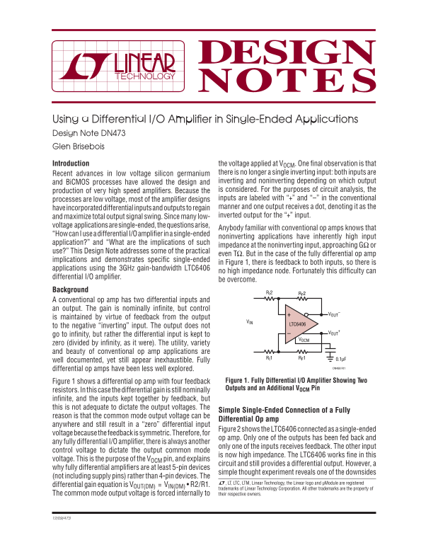
Figure 1 shows a differential op amp with four feedback Figure 1. Fully Differential I/O Amplifi er Showing Two Outputs and an Additional VOCM Pin
resistors. In this case the differential gain is still nominally infi nite, and the inputs kept together by feedback, but this is not adequate to dictate the output voltages. The
Simple Single-Ended Connection of a Fully
reason is that the common mode output voltage can be
Differential Op amp
anywhere and still result in a “zero” differential input
Figure 2 shows the LTC6406 connected as a single-ended
voltage because the feedback is symmetric. Therefore, for
op amp. Only one of the outputs has been fed back and
any fully differential I/O amplifi er, there is always another
only one of the inputs receives feedback. The other input
control voltage to dictate the output common mode
is now high impedance. The LTC6406 works fi ne in this
voltage. This is the purpose of the VOCM pin, and explains
circuit and still provides a differential output. However, a
why fully differential amplifi ers are at least 5-pin devices
simple thought experiment reveals one of the downsides
(not including supply pins) rather than 4-pin devices. The
L, LT, LTC, LTM, Linear Technology, the Linear logo and μModule are registered
differential gain equation is VOUT(DM) = VIN(DM) • R2/R1.
trademarks of Linear Technology Corporation. All other trademarks are the property of
The common mode output voltage is forced internally to their respective owners.
Page Summary Contents For LINEAR Design Note DN473: Using a Differential I/O Amplifier in Single-Ended Applications
Manual Details
| Brand | Linear |
|---|---|
| Pages | 2 |
| File Size | 95.42 KB |
| Published | June 17, 2026 |
Enter the captcha to get the download link:

Frequently Asked Questions
How can I use a differential amplifier in single-ended mode?
You must take the output from the closed loop path, which leaves one input high impedance for operation.
Is single-ended feedback detrimental to performance?
Yes; single-ended configuration introduces substantial noise gain on the open-loop output.
What is the operating bandwidth of the closed loop signal?
The single-ended closed loop output provides a specified 3dB bandwidth of 1.2 GHz.
How can I reduce input current noise in my system?
Buffering the device's input, for example with a JFET stage, drastically helps mitigate current noise effects.