Fairchild NC7SP00 Data Handbook (2)
Summary
The NC7SP00 is an Ultra Low Power (ULP) 2-input NAND Gate designed for applications where extending battery life is critical. Operating efficiently across a wide voltage range of 0.9V to 3.6V, this gate utilizes advanced CMOS technology to ensure minimal static and dynamic power dissipation. This manual serves as a comprehensive technical resource, detailing electrical characteristics, recommended operating conditions, packaging options (SC70 and MicroPak), logic functionality, and absolute safety ratings. It is specifically intended for engineers designing battery-powered circuits requiring exceptional energy efficiency and reliable low-voltage switching performance.
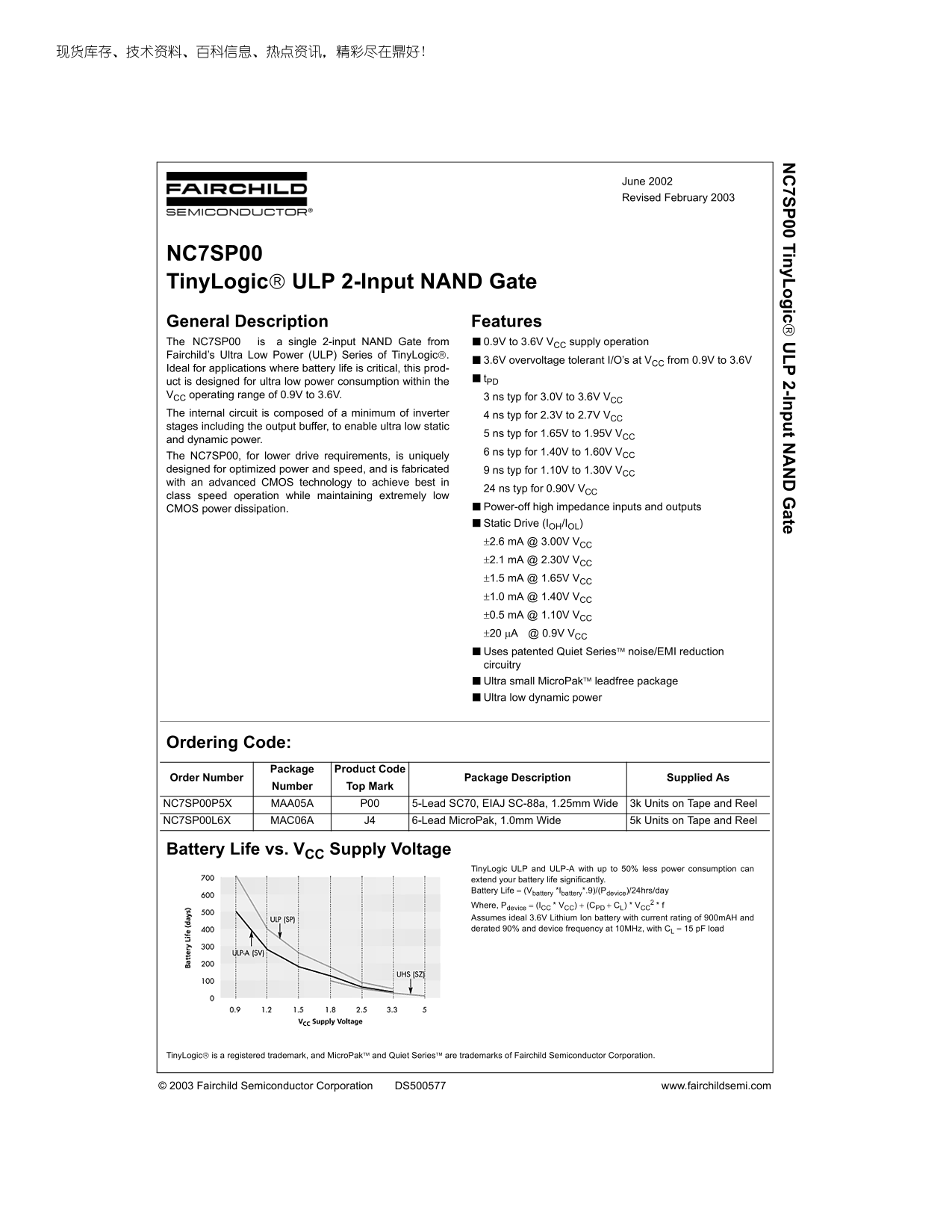
Page 1 Text Content
7S 00 Tin y L ic 2-In t N ate
June 2002 Revised February 2003
NC7SP00 Tiny Logic ULP 2-Input NAND Gate General Description Features The NC7SP00 is a single 2-input NAND Gate from ■0.9V to 3.6V VCC supply operation Fairchild’s Ultra Low Power (ULP) Series of Tiny Logic.
■3.6V overvoltage tolerant I/O’s at VCC from 0.9V to 3.6V
Ideal for applications where battery life is critical, this prod-
uct is designed for ultra low power consumption within the t PD
VCC operating range of 0.9V to 3.6V. 3 ns typ for 3.0V to 3.6V VCC The internal circuit is composed of a minimum of inverter 4 ns typ for 2.3V to 2.7V VCC stages including the output buffer, to enable ultra low static
5 ns typ for 1.65V to 1.95V VCC
and dynamic power.
6 ns typ for 1.40V to 1.60V VCC
The NC7SP00, for lower drive requirements, is uniquely designed for optimized power and speed, and is fabricated 9 ns typ for 1.10V to 1.30V VCC with an advanced CMOS technology to achieve best in
24 ns typ for 0.90V VCC
class speed operation while maintaining extremely low
CMOS power dissipation. ■Power-off high impedance inputs and outputs ■Static Drive (IOH/IOL) ±2.6 m A @ 3.00V VCC ±2.1 m A @ 2.30V VCC ±1.5 m A @ 1.65V VCC ±1.0 m A @ 1.40V VCC ±0.5 m A @ 1.10V VCC ±20 µA @ 0.9V VCC ■Uses patented Quiet Series noise/EMI reduction circuitry ■Ultra small Micro Pak leadfree package ■Ultra low dynamic power
Ordering Code:
Package Product Code
Order Number Package Description Supplied As
Number Top Mark
NC7SP00P5X MAA05A P00 5-Lead SC70, EIAJ SC-88a, 1.25mm Wide 3k Units on Tape and Reel NC7SP00L6X MAC06A J4 6-Lead Micro Pak, 1.0mm Wide 5k Units on Tape and Reel
Battery Life vs. VCC Supply Voltage
Tiny Logic ULP and ULP-A with up to 50% less power consumption can extend your battery life significantly. Battery Life = (Vbattery *Ibattery*.9)/(Pdevice)/24hrs/day
Where, Pdevice = (ICC * VCC) + (CPD + CL) * VCC Assumes ideal 3.6V Lithium Ion battery with current rating of 900m AH and derated 90% and device frequency at 10MHz, with CL = 15 p F load
Tiny Logic is a registered trademark, and Micro Pak and Quiet Series are trademarks of Fairchild Semiconductor Corporation.
© 2003 Fairchild Semiconductor Corporation DS500577 www.fairchildsemi.com
Page Summary Contents For Fairchild NC7SP00 Data Handbook (2)
Manual Details
| Brand | Fairchild |
|---|---|
| Pages | 9 |
| File Size | 322.45 KB |
| Published | July 06, 2026 |
Enter the captcha to get the download link:

Frequently Asked Questions
What is the operating voltage range for this NAND gate?
The recommended operating condition supply voltage is between 0.9V to 3.6V.
Is this circuit designed for low power consumption?
Yes, it is specifically designed to be ideal for applications where battery life is critical due to its ultra-low power features.
Are there package options available for the NC7SP00?
Yes, it is supplied in 5-Lead SC70 (MAA05A) and 6-Lead MicroPak (MAC06A) packages.
What are the general physical dimensions of the package?
The SC70 package has a width of 1.25mm, while the MicroPak package is 1.0mm wide.