Fairchild MM74C906 3669 Hex Open Drain N-Channel Buffers, MM74C907 3660 Hex Open Drain P-Channel Buffers Data Manual
Summary
The MM74C906 and MM74C907 are high-performance, open drain buffer ICs designed for signal conditioning, level shifting, and creating wire AND/OR logic gates. These chips operate across a wide supply voltage range (3V to 15V), offering both N-channel (MM74C906) and P-channel (MM74C907) solutions. This manual provides comprehensive technical data, including electrical characteristics, absolute maximum ratings, propagation delays, and detailed connection diagrams for integration into robust electronic circuits. Ideal for engineers needing stable, high-current buffering in complex digital systems.
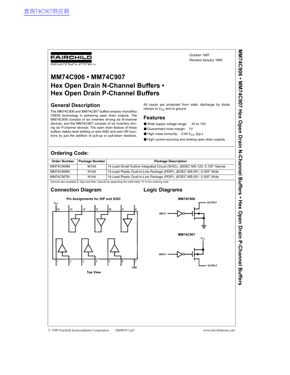
Page 1 Text Content
74C 906 • M 74C 907 H ex O en rain -C an el B ffers • H ex O en rain -C an el B ffers
October 1987 Revised January 1999
MM74C906 • MM74C907 Hex Open Drain N-Channel Buffers • Hex Open Drain P-Channel Buffers
All inputs are protected from static discharge by diode
General Description
clamps to VCC and to ground.
The MM74C906 and MM74C907 buffers employ monolithic CMOS technology in achieving open drain outputs. The
Features
MM74C906 consists of six inverters driving six N-channel devices; and the MM74C907 consists of six inverters driv- Wide supply voltage range: 3V to 15V ing six P-channel devices. The open drain feature of these
Guaranteed noise margin: 1V
buffers makes level shifting or wire AND and wire OR func-
High noise immunity: 0.45 VCC (typ.)
tions by just the addition of pull-up or pull-down resistors.
High current sourcing and sinking open drain outputs
Ordering Code: Order Number Package Number Package Description MM74C906M M14A 14-Lead Small Outline Integrated Circuit (SOIC), JEDEC MS-120, 0.150” Narrow MM74C906N N14A 14-Lead Plastic Dual-In-Line Package (PDIP), JEDEC MS-001, 0.300” Wide MM74C907N N14A 14-Lead Plastic Dual-In-Line Package (PDIP), JEDEC MS-001, 0.300” Wide Devices also available in Tape and Reel. Specify by appending the suffix letter “X” to the ordering code.
Connection Diagram Logic Diagrams Pin Assignments for DIP and SOIC MM74C906
MM74C907
Top View
© 1999 Fairchild Semiconductor Corporation DS005911.prf www.fairchildsemi.com
Page Summary Contents For Fairchild MM74C906 3669 Hex Open Drain N-Channel Buffers, MM74C907 3660 Hex Open Drain P-Channel Buffers Data Manual
Manual Details
| Brand | Fairchild |
|---|---|
| Pages | 5 |
| File Size | 54.28 KB |
| Published | May 30, 2026 |
Enter the captcha to get the download link:

Frequently Asked Questions
What type of output do these buffers utilize?
They employ open drain outputs, which allows for level shifting or connecting via pull-up/down resistors.
What are the operational voltage limits for the input pins?
The voltage at any input pin must remain between -0.3V and +0.3V.
Are these chips compatible with both CMOS and TTL logic levels?
Yes, they support interfaces from CMOS or TTL to PMOS, or CMOS or TTL to CMOS.
How can I order the wide package version of these devices?
You must specify by appending the suffix letter 'X' to the corresponding ordering code (MM74C906N or MM74C907N).