Fairchild FST3345 Data Handbook
Summary
The FST3345 is a high-speed, CMOS TTL-compatible 8-bit bus switch designed to reliably connect or disconnect signals between two ports with minimal propagation delay. This component allows for precise control over data routing in complex electronic systems using simple enable inputs. The accompanying manual provides comprehensive technical specifications, including detailed electrical characteristics, operating guidelines, and various package options (SOIC, QSOP, TSSOP). It is essential reading for hardware engineers and system designers integrating reliable, low-resistance bus switching components into their circuit boards.
Page 1 Text Content
查询FST3345供应商
3345 8-B it B s S itch
June 1997 Revised December 1999
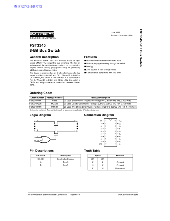
FST3345 8-Bit Bus Switch General Description Features The Fairchild Switch FST3345 provides 8-bits of high- ■4Ω switch connection between two ports. speed CMOS TTL-compatible bus switching. The low on
■Minimal propagation delay through the switch.
resistance of the switch allows inputs to be connected to
■Low l CC.
outputs without adding propagation delay or generating
additional ground bounce noise. ■Zero bounce in flow-through mode. The device is organized as an 8-bit switch bank with dual ■Control inputs compatible with TTL level.
output enable inputs (OE and OE). When OE is LOW or OE is HIGH, the switch is ON and Port A is connected to Port B. When OE is HIGH and OE is LOW, the switch is OPEN and a high-impedance state exists between the two ports.
Ordering Code: Order Number Package Number Package Description FST3345WM M20B 20-Lead Small Outline Integrated Circuit (SOIC), JEDEC MS-013, 0.300 Wide FST3345QSC MQA20 20-Lead Quarter Size Outline Package (QSOP), JEDEC MO-137, 0.150 Wide FST3345MTC MTC20 20-Lead Thin Shrink Small Outline Package (TSSOP), JEDEC MO-153, 4.4mm Wide Devices also available in Tape and Reel. Specify by appending the suffix letter “X” to the ordering code.
Logic Diagram Connection Diagram
Pin Descriptions Truth Table Pin Name Description Inputs Function OE, OE Bus Switch Enables OE OE
Bus A Connect Bus B Connect
Disconnect
© 1999 Fairchild Semiconductor Corporation DS500019 www.fairchildsemi.com
Page Summary Contents For Fairchild FST3345 Data Handbook
Manual Details
| Brand | Fairchild |
|---|---|
| Pages | 6 |
| File Size | 118.49 KB |
| Published | June 03, 2026 |
Enter the captcha to get the download link:
