Fairchild FDC5614P Product Specificationsheet
Summary
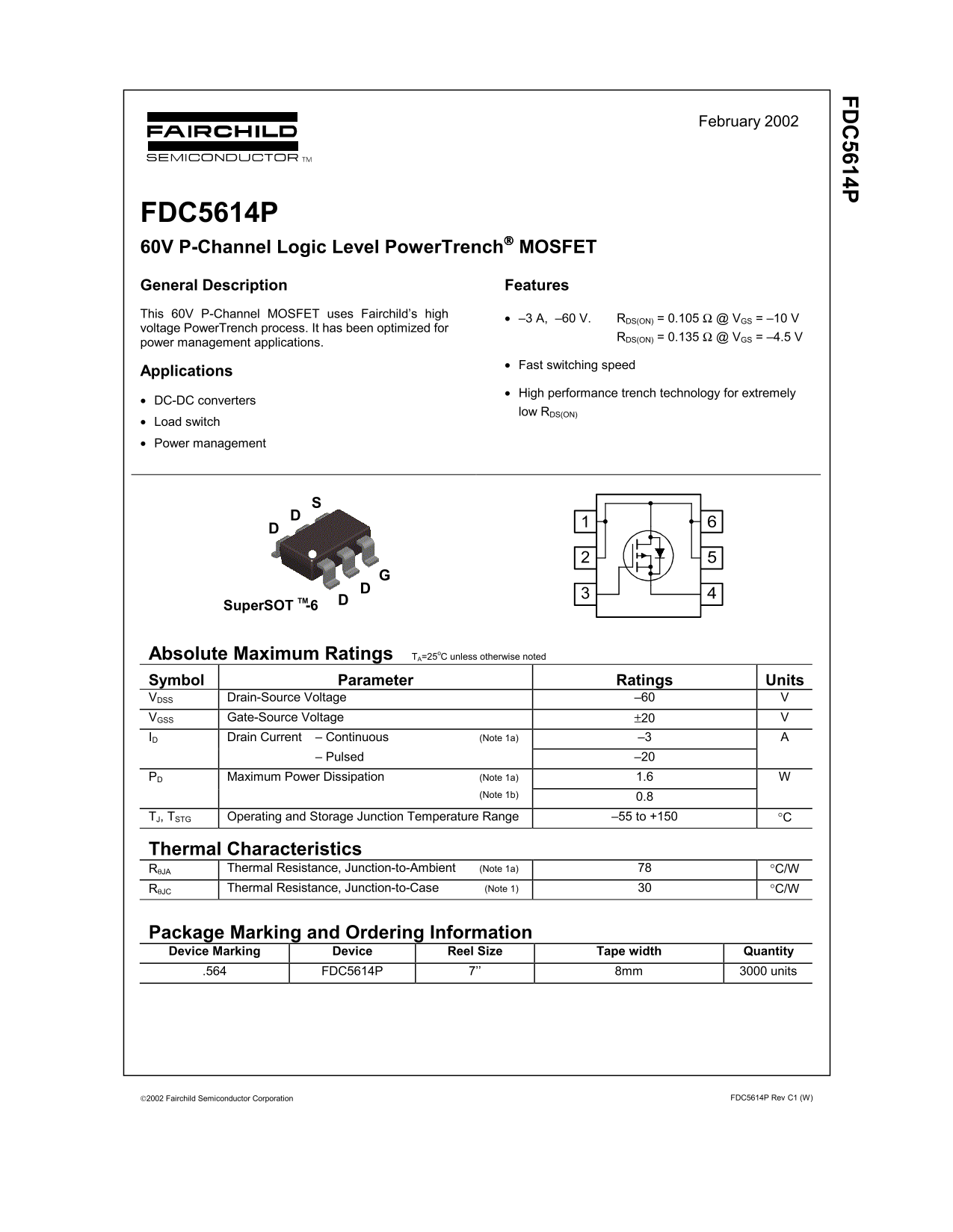
Fairchild Semiconductor FDC5614P 60V P-Channel Logic Level PowerTrench MOSFET datasheet (February 2002) documenting this -3A, -60V P-channel MOSFET in SuperSOT-6 package. Features low RDS(ON) of 0.105 ohm at VGS=-10V and 0.135 ohm at VGS=-4.5V for logic-level gate drive, gate threshold voltage of -1.0 to -3.0V, and fast switching speed. Thermal resistance: 78C/W junction-to-ambient, 30C/W junction-to-case. Maximum power dissipation 1.6W. Designed for DC-DC converters, load switches, and power ma
Page 1 Text Content
FD 5614P
February 2002
FDC5614P 60V P-Channel Logic Level Power Trench MOSFET General Description Features This 60V P-Channel MOSFET uses Fairchild’s high
• –3 A, –60 V. RDS(ON) = 0.105 Ω @ VGS = –10 V
voltage Power Trench process. It has been optimized for
RDS(ON) = 0.135 Ω @ VGS = –4.5 V
power management applications.
• Fast switching speed
Applications
• High performance trench technology for extremely
• DC-DC converters
low RDS(ON)
• Load switch • Power management
Super SOT -6TM
Absolute Maximum Ratings TA=25o C unless otherwise noted Symbol Parameter Ratings Units VDSS Drain-Source Voltage –60 V VGSS Gate-Source Voltage ±20 V ID Drain Current – Continuous (Note 1a) –3 A – Pulsed –20
Maximum Power Dissipation (Note 1a) 1.6 W PD (Note 1b) 0.8
TJ, TSTG Operating and Storage Junction Temperature Range –55 to +150 °C
Thermal Characteristics RθJA Thermal Resistance, Junction-to-Ambient (Note 1a) 78 °C/W RθJC Thermal Resistance, Junction-to-Case (Note 1) 30 °C/W
Package Marking and Ordering Information Device Marking Device Reel Size Tape width Quantity .564 FDC5614P 7’’ 8mm 3000 units
2002 Fairchild Semiconductor Corporation FDC5614P Rev C1 (W)
Page Summary Contents For Fairchild FDC5614P Product Specificationsheet
Manual Details
| Brand | Fairchild |
|---|---|
| Pages | 5 |
| File Size | 140.43 KB |
| Published | July 06, 2026 |
Enter the captcha to get the download link:

Frequently Asked Questions
What are the typical applications for this P-Channel MOSFET?
It is optimized for power management applications, including DC-DC converters and load switches.
Is this component cleared for use in critical life support devices?
No. It is not authorized for use as a critical component in life support systems without explicit written approval from Fairchild Semiconductor Corporation.
What is the typical Drain-Source On-Resistance at 25°C?
The typical Rds(on) is listed as 82 mΩ when tested at V = -10V and I = -3A.