FAIRCHILD 74VHC4051, 74VHC4052, 74VHC4053 8-Channel Analog Multiplexer, Dual 4-Channel Analog Multiplexer, Triple 2-Channel Analog Multiplexer Owner's Manual and User Guide
Summary
These integrated circuits offer high-performance, digitally controlled analog multiplexers for signal switching. Available in configurations ranging from single 8-channel up to triple 2-channel setups, these switches excel at routing varying analog signals (±6V) using low-resistance CMOS technology. The accompanying manual provides comprehensive technical details—including electrical specifications, functional logic diagrams, and multiple package options—making it the essential resource for hardware engineers and designers implementing robust, multi-signal switching systems in their electronics.
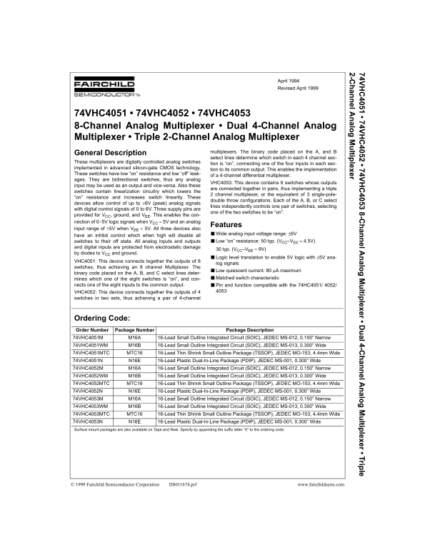
Page 1 Text Content
74V 4051 • 74V 4052 • 74V 4053 8-C an el A alo ltip lexer • D al 4-C an el A alo ltip lexer • Trip le 2-C an el A alo ltip lexer
April 1994 Revised April 1999
74VHC4051 • 74VHC4052 • 74VHC4053 8-Channel Analog Multiplexer • Dual 4-Channel Analog Multiplexer • Triple 2-Channel Analog Multiplexer
multiplexers. The binary code placed on the A, and B
General Description
select lines determine which switch in each 4 channel sec-
These multiplexers are digitally controlled analog switches
tion is “on”, connecting one of the four inputs in each sec-
implemented in advanced silicon-gate CMOS technology.
tion to its common output. This enables the implementation
These switches have low “on” resistance and low “off” leak-
of a 4-channel differential multiplexer.
ages. They are bidirectional switches, thus any analog
VHC4053: This device contains 6 switches whose outputs
input may be used as an output and vice-versa. Also these
are connected together in pairs, thus implementing a triple
switches contain linearization circuitry which lowers the
2 channel multiplexer, or the equivalent of 3 single-pole-
“on” resistance and increases switch linearity. These
double throw configurations. Each of the A, B, or C select
devices allow control of up to ±6V (peak) analog signals
lines independently controls one pair of switches, selecting
with digital control signals of 0 to 6V. Three supply pins are
one of the two switches to be “on”.
provided for VCC, ground, and VEE. This enables the con- nection of 0–5V logic signals when VCC = 5V and an analog
Features
input range of ±5V when VEE = 5V. All three devices also
Wide analog input voltage range: ±6V
have an inhibit control which when high will disable all
switches to their off state. All analog inputs and outputs Low “on” resistance: 50 typ. (VCC–VEE = 4.5V)
and digital inputs are protected from electrostatic damage
30 typ. (VCC–VEE = 9V)
by diodes to VCC and ground.
Logic level translation to enable 5V logic with ±5V ana-
VHC4051: This device connects together the outputs of 8
log signals
switches, thus achieving an 8 channel Multiplexer. The
Low quiescent current: 80 µA maximum
binary code placed on the A, B, and C select lines deter-
mines which one of the eight switches is “on”, and con- Matched switch characteristic
nects one of the eight inputs to the common output. Pin and function compatible with the 74HC4051/ 4052/ VHC4052: This device connects together the outputs of 4 switches in two sets, thus achieving a pair of 4-channel
Ordering Code: Order Number Package Number Package Description 74VHC4051M M16A 16-Lead Small Outline Integrated Circuit (SOIC), JEDEC MS-012, 0.150” Narrow 74VHC4051WM M16B 16-Lead Small Outline Integrated Circuit (SOIC), JEDEC MS-013, 0.300” Wide 74VHC4051MTC MTC16 16-Lead Thin Shrink Small Outline Package (TSSOP), JEDEC MO-153, 4.4mm Wide 74VHC4051N N16E 16-Lead Plastic Dual-In-Line Package (PDIP), JEDEC MS-001, 0.300” Wide 74VHC4052M M16A 16-Lead Small Outline Integrated Circuit (SOIC), JEDEC MS-012, 0.150” Narrow 74VHC4052WM M16B 16-Lead Small Outline Integrated Circuit (SOIC), JEDEC MS-013, 0.300” Wide 74VHC4052MTC MTC16 16-Lead Thin Shrink Small Outline Package (TSSOP), JEDEC MO-153, 4.4mm Wide 74VHC4052N N16E 16-Lead Plastic Dual-In-Line Package (PDIP), JEDEC MS-001, 0.300” Wide 74VHC4053M M16A 16-Lead Small Outline Integrated Circuit (SOIC), JEDEC MS-012, 0.150” Narrow 74VHC4053WM M16B 16-Lead Small Outline Integrated Circuit (SOIC), JEDEC MS-013, 0.300” Wide 74VHC4053MTC MTC16 16-Lead Thin Shrink Small Outline Package (TSSOP), JEDEC MO-153, 4.4mm Wide 74VHC4053N N16E 16-Lead Plastic Dual-In-Line Package (PDIP), JEDEC MS-001, 0.300” Wide Surface mount packages are also available on Tape and Reel. Specify by appending the suffix letter “X” to the ordering code.
© 1999 Fairchild Semiconductor Corporation DS011674.prf www.fairchildsemi.com
Page Summary Contents For FAIRCHILD 74VHC4051, 74VHC4052, 74VHC4053 8-Channel Analog Multiplexer, Dual 4-Channel Analog Multiplexer, Triple 2-Channel Analog Multiplexer Owner's Manual and User Guide
Manual Details
| Brand | Fairchild |
|---|---|
| Pages | 11 |
| File Size | 108.94 KB |
| Published | May 19, 2026 |
Enter the captcha to get the download link:

Frequently Asked Questions
What is the recommended operating supply voltage range?
The typical supply voltage range is 5V (CC) with an analog input voltage range of ±6V.
Do these multiplexers have low power consumption?
Yes, they feature low quiescent current and low ‘on’ resistance (e.g., 50 typ. Ω for 4V–9V).
What protection is offered against electrical damage?
All analog inputs and outputs are protected from electrostatic damage by diodes to V and ground.
Are these switches bidirectional?
Yes, they are bidirectional switches; any given analog input may be used as an output and vice-versa.