Fairchild 74VCX32244 Low Voltage 32-Bit Buffer Line Driver with 3.6V Tolerant Inputs and Outputs - Data Sheet
Summary
This high-performance 32-bit buffer/line driver is engineered for modern low-voltage digital applications operating between 1.2V and 3.6V. Featuring thirty-two non-inverting buffers with advanced 3-STATE outputs, the component provides robust signal integrity, along with superior noise/EMI reduction circuitry. This manual details device functionality, electrical specifications (ratings and safe operating limits), connectivity diagrams, and full implementation guidelines for engineers designing reliable digital bus or clock driver systems requiring high tolerance levels.
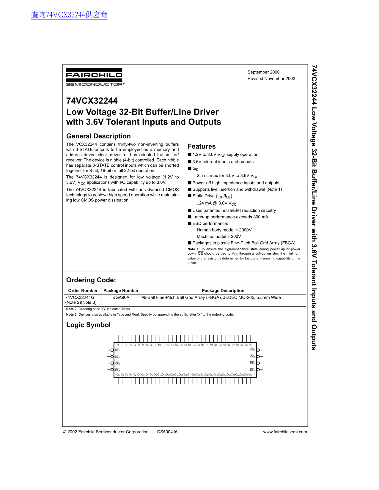
Page 1 Text Content
查询74VCX32244供应商
74V 32244 L Vo ltag e 32-B it B ffer/L in e D river w ith 3.6V To leran t In ts an tp ts
September 2000 Revised November 2002
74VCX32244 Low Voltage 32-Bit Buffer/Line Driver with 3.6V Tolerant Inputs and Outputs General Description The VCX32244 contains thirty-two non-inverting buffers
Features
with 3-STATE outputs to be employed as a memory and
address driver, clock driver, or bus oriented transmitter/ ■1.2V to 3.6V VCC supply operation
receiver. The device is nibble (4-bit) controlled. Each nibble
■3.6V tolerant inputs and outputs
has separate 3-STATE control inputs which can be shorted
together for 8-bit, 16-bit or full 32-bit operation.
2.5 ns max for 3.0V to 3.6V VCC
The 74VCX32244 is designed for low voltage (1.2V to 3.6V) VCC applications with I/O capability up to 3.6V. ■Power-off high impedance inputs and outputs
The 74VCX32244 is fabricated with an advanced CMOS ■Supports live insertion and withdrawal (Note 1)
technology to achieve high speed operation while maintain- ■Static Drive (IOH/IOL) ing low CMOS power dissipation.
±24 m A @ 3.0V VCC ■Uses patented noise/EMI reduction circuitry ■Latch-up performance exceeds 300 m A ■ESD performance: Human body model > 2000V Machine model > 200V ■Packages in plastic Fine-Pitch Ball Grid Array (FBGA) Note 1: To ensure the high-impedance state during power up or power down, OE should be tied to VCC through a pull-up resistor; the minimum value of the resistor is determined by the current-sourcing capability of the driver.
Ordering Code: Order Number Package Number Package Description 74VCX32244G BGA96A 96-Ball Fine-Pitch Ball Grid Array (FBGA), JEDEC MO-205, 5.5mm Wide (Note 2)(Note 3) Note 2: Ordering code “G” indicates Trays. Note 3: Devices also available in Tape and Reel. Specify by appending the suffix letter “X” to the ordering code.
Logic Symbol
© 2002 Fairchild Semiconductor Corporation DS500416 www.fairchildsemi.com
Page Summary Contents For Fairchild 74VCX32244 Low Voltage 32-Bit Buffer Line Driver with 3.6V Tolerant Inputs and Outputs - Data Sheet
Manual Details
| Brand | Fairchild |
|---|---|
| Pages | 9 |
| File Size | 106.02 KB |
| Published | July 12, 2026 |
Enter the captcha to get the download link:

Frequently Asked Questions
What is the recommended operating voltage range for this buffer/line driver?
The device operates at low voltages, specifically from 1.2V to 3.6V.
Does the 74VCX32244 have high-speed features or advanced technology?
Yes, it includes an advanced CMOS fabric and Supports 'live insertion and withdrawal' technology for high speed while maintaining low power dissipation.
How is full 32-bit operation achieved?
Full 32-bit operation can be achieved by shorting separate 3-STATE control inputs together in a nibble (4-bit) block, allowing the device to be fully controlled.
Are there specific requirements for the Output Enable (OE) input during power changes?
To ensure high-impedance state during power up or power down, OE must be tied to V through a pull-up resistor with a minimum current value set by the driver's current-sourcing capability.