# A B C D E F G H I J K L M N O P Q R S T U V W X Y Z

ATMEL ATF1502AS Preliminary Data Handbook

Summary

The ATF1502AS is a high-performance, high-density Complex Programmable Logic Device (CPLD) designed for robust digital control and signal processing. This technical manual provides comprehensive coverage of the device's architecture, featuring advanced concepts such as 4 plex logic macrocells, up to 32 I/O pins, and integrated EEPROM technology. It details crucial operational specifications, including JTAG Boundary Scan compatibility and specialized power management options. This product is essential for electrical engineers and hardware designers building sophisticated digital systems that require flexible, high-speed, and reliable programmable logic integration.
📄 Preview PAGE OF 18

Page 1 Text Content

查询ATF1502AS供应商

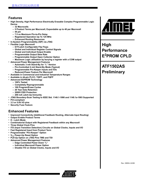
Features High Density, High Performance Electrically Erasable Complex Programmable Logic Device 32 Macrocells 5 Product Terms per Macrocell, Expandable up to 40 per Macrocell 44 pin 7.5 ns Maximum Pin-to-Pin Delay Registered Operation Up To 125 MHz Enhanced Routing Resources In-System Programmability (ISP) via JTAG Flexible Logic Macrocell High D/T/Latch Configurable Flip Flops Global and Individual Register Control Signals

Performance

Global and Individual Output Enable Programmable Output Slew Rate

Programmable Output Open Collector Option E2PROM CPLD

Maximum Logic utilization by burying a register with a COM output Advanced Power Management Features Automatic 3 m A Stand-By for “L” Version

Pin-Controlled 4 m A Stand-By Mode (Typical) ATF1502AS

Programmable Pin-Keeper Inputs and I/Os Reduced-Power Feature Per Macrocell Preliminary Available in Commercial and Industrial Temperature Ranges Available in 44-pin PLCC; TQFP; and PQFP Advanced EEPROM Technology 100% Tested Completely Reprogrammable 100 Program/Erase Cycles 20 Year Data Retention 2000V ESD Protection 200 m A Latch-Up Immunity JTAG Boundary-Scan Testing to IEEE Std. 1149.1-1990 and 1149.1a-1993 Supported PCI-compliant 3.3 or 5.0V I/O pins Security Fuse Feature

Enhanced Features Improved Connectivity (Additional Feedback Routing, Alternate Input Routing) Output Enable Product Terms D - Latch Mode Combinatorial Output with Registered Feedback within any Macrocell Three Global Clock Pins ITD (Input Transition Detection) Circuits on Global Clocks, Inputs and I/O Fast Registered Input from Product Term Programmable “Pin-Keeper” Option VCC Power-Up Reset Option Pull-Up Option on JTAG Pins TMS and TDI Advanced Power Management Features Edge Controlled Power Down “L” Individual Macrocell Power Option Disable ITD on Global Clocks, Inputs and I/O

Rev. 0995A–04/98

Page Summary Contents For ATMEL ATF1502AS Preliminary Data Handbook

Page 1 查询ATF1502AS供应商 Features High Density, High Performance Electrically Erasable Complex Programmable Logic Device 32 Macrocells 5 Product Terms per Macrocell, Expandable up to 40 per Macrocell 44 pin 7.5...
Page 2 44-Lead TQFP/PQFP 44-Lead PLCC Top View Top View I/O I/O I/O I/O I/O I/O /P I/O /P TDI/I/O I/O I/O/TDI I/O I/O 2/ I/O I/O/TDO I/O I/O/TDO LR /I GND I/O GND I/O 1/ PD1/I/O VCC PD1/I/O I/O VCC I/O I/O I...
Page 3 ATF1502AS Each macrocell also generates a foldback logic term, which when programmed, ro tec ts the contents the goes to a regional bus. Cascade logic between macrocells ATF1502AS. Two bytes (16-bits)...
Page 4 macrocell. (This feature is automatically implemented by This circuitry prevents unused input and I/O lines from the fitter software). In addition to D, T, JK and SR opera- floating to intermediate vo...
Page 5 ATF1502AS option is selected in the design source file. When enabled, 1. The VCC rise must be monotonic, the device goes into power down when either PD1 or PD2 2. After reset occurs, all input and fee...
Page 6 JTAG-BST/ISP Overview BSC Configuration for Input and I/O The JTAG boundary-scan testing is controlled by the Test Pins (except JTAG TAP Pins) Access Port (TAP) controller in the ATF1502AS. The bounda...
Page 7 ATF1502AS DC Characteristics Symbol Parameter Condition Min Typ Max Units Input or I/O Low IIL VIN = VCC -2 -10 µA Leakage Current Input or I/O High Leakage Current Tri-State Output IOZ VO = VCC or GN...
Page 8 Absolute Maximum Ratings* Temperature Under Bias.................................. -40°C to +85°C *NOTICE: Stresses beyond those listed under “Absolute Maximum Ratings” may cause permanent dam- Storag...
Page 9 ATF1502AS AC Characteristics (Continued) Symbol Parameter Max Min Max Min Max Min Max Min Max Units Min FMAX Maximum Clock Frequency 166.7 83.3 MHz t IN Input Pad and Buffer Delay 0.5 0.5 ns t IO I/O ...
Page 10 AC Characteristics (Continued) Symbol Parameter Max Min Max Min Max Min Max Min Max Units Min Output Buffer Enable Delay t ZX1 (Slow slew rate = OFF; 4.0 5.0 ns VCCIO = 5.0V; CL = 35 p F) Output Buffe...
Page 11 ATF1502AS Power Down Mode The ATF1502AS includes an optional pin controlled power signals except the power down pin are blocked. Input and down feature.When this mode is enabled, the PD pin acts I/O h...
Page 12 BSC Configuration for Mac BSC for Dedicated Input Capture DR TDI Clock Shift TDICLOCK Capture Update DR DR TDI Mode Shift Clock BSC for I/O Pins and Macrocells ATF1502AS12
Page 13 ATF1502AS PCI Compliance high current load required by the PCI interface. The ATF1502AS allows this without contributing to system The ATF1502AS also supports the growing need in the noise while deliv...
Page 14 PCI DC Characteristics (Preliminary) Symbol Parameter Conditions Min Max Units VCC Supply Voltage 4.75 5.25 VIH Input High Voltage 2.0 VCC + 0.5 VIL Input Low Voltage -0.5 0.8 IIH Input High Leakage C...
Page 15 ATF1502AS ATF1502AS Dedicated Pinouts 44-Pin 44-Pin 44-Pin Dedicated Pin TQFP J-Lead PQFP INPUT/OE2/GCLK2 INPUT/GCLR INPUT/OE1 INPUT/GCLK1 I/O /GCLK3 I/O / PD (1,2) 5, 19 11, 25 5, 19 I/O / TDI (JTAG)...
Page 16 ATF1502AS I/O Pinouts MC PLC 44-Pin PLCC 44-Pin TQFP 44-Pin PQFP A/PD1 8/TDI 32/TMS ATF1502AS16
Page 17 ATF1502AS Ordering Information t PD t CO1 f MAX (ns) (ns) (MHz) Ordering Code Package Operation Range 7.5 4.5 166.7 ATF1502AS-7 AC44 44A Commercial ATF1502AS-7 JC44 44J (0°C to 70°C) ATF1502AS-7 QC44 ...
Page 18 Packaging Information 44A, 44-Lead, Thin (1.0 mm) Plastic Gull Wing 44J, 44-Lead, Plastic J-Leaded Chip Carrier (PLCC) Quad Flat Package (TQFP) Dimensions in Inches and (Millimeters) Dimensions in Mil...

Manual Details

Brand Atmel
Pages 18
File Size 348.77 KB
Published May 15, 2026
187 views

Enter the captcha to get the download link:

captcha

Frequently Asked Questions

How can I program or test this CPLD?

It is In-System Programmable (ISP) via JTAG, and supports Boundary-Scan Testing to IEEE Std. 1149.1.

What are the available operating temperatures?

The ATF1502AS comes in both Commercial ranges (0°C to 70°C) and Industrial ranges (-40°C to +85°C).

How does this device manage power consumption when idle?

It supports automatic 3 mA Stand-By for the 'L' version, or pin-controlled 4 mA standby mode.

What I/O voltage standards are supported?

The device supports both 3.3V or 5.0V signal output pins.