# A B C D E F G H I J K L M N O P Q R S T U V W X Y Z

ATMEL AT49BV160DT Data Handbook

Summary

This 16-megabit Flash memory solution is designed for reliable, in-system programming requiring single voltage read/write operation. Featuring robust sector erase architecture and critical data protection via suspend/resume capabilities, it ensures stable data management even during complex write cycles. The technical manual provides comprehensive guidance covering command sequences, device operational modes (Read, Program, Erase), pin configurations, and timing requirements for electrical engineers integrating the chip into demanding electronic designs.
📄 Preview 📖 Table of Contents Contents PAGE OF 28

Page 1 Text Content

BDTIC www.BDTIC.com/ATMEL

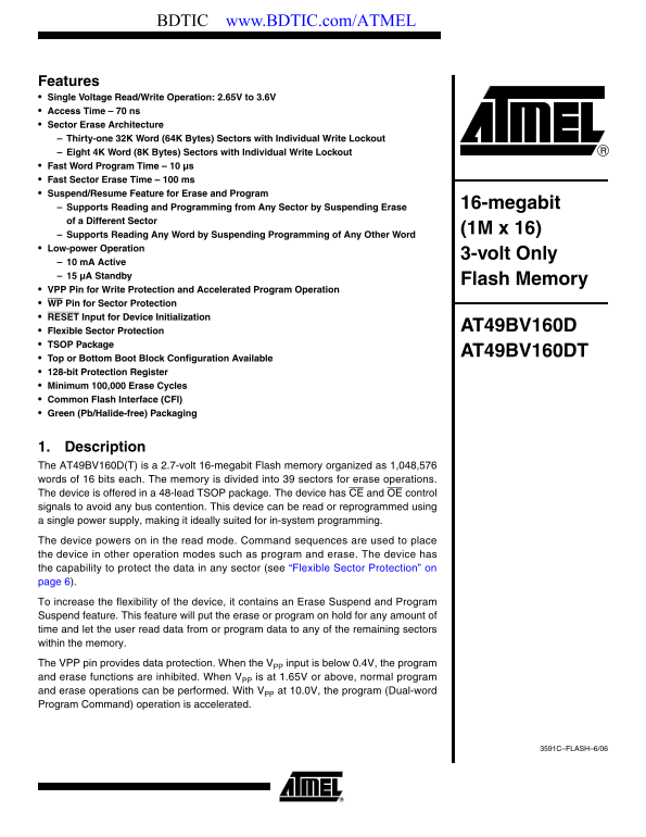
Features Single Voltage Read/Write Operation: 2.65V to 3.6V Access Time – 70 ns Sector Erase Architecture Thirty-one 32K Word (64K Bytes) Sectors with Individual Write Lockout Eight 4K Word (8K Bytes) Sectors with Individual Write Lockout Fast Word Program Time – 10 µs Fast Sector Erase Time – 100 ms Suspend/Resume Feature for Erase and Program

Supports Reading and Programming from Any Sector by Suspending Erase 16-megabit

of a Different Sector

Supports Reading Any Word by Suspending Programming of Any Other Word Low-power Operation

3-volt Only

10 m A Active 15 µA Standby

Flash Memory

VPP Pin for Write Protection and Accelerated Program Operation WP Pin for Sector Protection RESET Input for Device Initialization

AT49BV160D

Flexible Sector Protection TSOP Package

AT49BV160DT

Top or Bottom Boot Block Configuration Available 128-bit Protection Register Minimum 100,000 Erase Cycles Common Flash Interface (CFI) Green (Pb/Halide-free) Packaging

1. Description The AT49BV160D(T) is a 2.7-volt 16-megabit Flash memory organized as 1,048,576 words of 16 bits each. The memory is divided into 39 sectors for erase operations. The device is offered in a 48-lead TSOP package. The device has CE and OE control signals to avoid any bus contention. This device can be read or reprogrammed using a single power supply, making it ideally suited for in-system programming. The device powers on in the read mode. Command sequences are used to place the device in other operation modes such as program and erase. The device has the capability to protect the data in any sector (see “Flexible Sector Protection” on page 6). To increase the flexibility of the device, it contains an Erase Suspend and Program Suspend feature. This feature will put the erase or program on hold for any amount of time and let the user read data from or program data to any of the remaining sectors within the memory. The VPP pin provides data protection. When the VPP input is below 0.4V, the program and erase functions are inhibited. When VPP is at 1.65V or above, normal program and erase operations can be performed. With VPP at 10.0V, the program (Dual-word Program Command) operation is accelerated.

3591C–FLASH–6/06

Page Summary Contents For ATMEL AT49BV160DT Data Handbook

Page 1 BDTIC www.BDTIC.com/ATMEL Features Single Voltage Read/Write Operation: 2.65V to 3.6V Access Time – 70 ns Sector Erase Architecture Thirty-one 32K Word (64K Bytes) Sectors with Individual Write Lockou...
Page 2 2. Pin Configurations Pin Name Function A0 - A19 Addresses CE Chip Enable OE Output Enable WE Write Enable RESET Reset VPP Write Protection I/O0 - I/O15 Data Inputs/Outputs NC No Connect VCCQ Output P...
Page 3 AT49BV160D(T) 3. Block Diagram OUTPUT INPUT BUFFER BUFFER IDENTIFIER REGISTER TP LT IP LE INPUT BUFFER STATUS CE REGISTER WE COMMAND REGISTER RESET ADDRESS WP LATCH DATA COMPARATOR WRITE STATE MACHINE...
Page 4 4.3 Reset A RESET input pin is provided to ease some system applications. When RESET is at a logic high level, the device is in its standard operating mode. A low level on the RESET input halts the pr...
Page 5 AT49BV160D(T) 4.7 Read Status Register The status register indicates the status of device operations and the success/failure of that oper- ation. The Read Status Register command causes subsequent rea...
Page 6 4.7.1 Clear Status Register The WSM can set status register bits 1 through 7 and can clear bits 2, 6 and 7; but, the WSM cannot clear status register bits 1, 3, 4 or 5. Because bits 1, 3, 4 and 5 indi...
Page 7 AT49BV160D(T) Table 4-2. Hardlock and Softlock Protection Configurations in Conjunction with WP Erase/ Hard- Soft- Prog VPP WP lock lock Allowed? Comments VCC/5V Yes No sector is locked Sector is Soft...
Page 8 4.8.3 Sector Protection Detection A software method is available to determine if the sector protection Softlock or Hardlock features are enabled. When the device is in the software product identificat...
Page 9 AT49BV160D(T) 4.12 128-bit Protection Register The AT49BV160D(T) contains a 128-bit register that can be used for security purposes in sys- tem design. The protection register is divided into two 64-b...
Page 10 5. Word Program Flowchart 6. Word Program Procedure Start Operation Command Comments Program Data = 40 Write Setup Addr = Any Address Write 40, (Setup) Any Address Data = Data to program Write Data Ad...
Page 11 AT49BV160D(T) 9. Program Suspend/Resume 10. Program Suspend/Resume Flowchart Procedure Start Operation Command Comments Program Data = B0 Write Suspend Addr = Any Address Write B0 (Program Suspend) An...
Page 12 11. Sector Erase Flowchart 12. Sector Erase Procedure Start Operation Command Comments Sector Write 20, Data = 20 Sector Erase) Any Address Write Erase Addr = Any Address Setup Write D0, (Erase Confir...
Page 13 AT49BV160D(T) 15. Erase Suspend/Resume Flowchart 16. Erase Suspend/Resume Procedure Start Operation Command Comments Erase Data = B0 Write B0, Write (Erase Suspend) Any Address Suspend Addr = Any addr...
Page 14 17. Protection Register Programming 18. Protection Register Programming Flowchart Procedure Start Operation Command Comments Program Data = C0 Write C0, (Program-Setup) Write Any Address PR Setup Addr...
Page 15 AT49BV160D(T) 21. Command Definition Table 1st Bus Cycle 2nd Bus Cycle 3rd Bus Cycle Command Sequence Cycles Addr Data Addr Data Addr Data Read XX FF Sector Erase/Confirm XX SA(2) D0 Word Program XX 4...
Page 16 23. Protection Register Addressing Table Word Use Sector A7 A6 A5 A4 A3 A2 A1 A0 Factory Factory Factory Factory User User User User Note: All address lines not specified in the above table must be “0...
Page 17 AT49BV160D(T) 24. AT49BV160D – Sector Address Table Sector Size (Bytes/Words) Address Range (A19 - A0) SA0 8K/4K 00000 - 00FFF SA1 8K/4K 01000 - 01FFF SA2 8K/4K 02000 - 02FFF SA3 8K/4K 03000 - 03FFF S...
Page 18 25. AT49BV160DT – Sector Address Table Sector Size (Bytes/Words) Address Range (A19 - A0) SA0 64K/32K 00000 - 07FFF SA1 64K/32K 08000 - 0FFFF SA2 64K/32K 10000 - 17FFF SA3 64K/32K 18000 - 1FFFF SA4 64...
Page 19 AT49BV160D(T) 26. DC and AC Operating Range AT49BV160D(T)-70 Operating Temperature (Case) Ind. -40°C - 85°C VCC Power Supply 2.65V to 3.6V 27. Operating Modes Mode CE OE WE RESET VPP Ai I/O Read VIL V...
Page 20 29. Input Test Waveforms and Measurement Level t R, t F < 5 ns 30. Output Test Load 31. Pin Capacitance f = 1 MHz, T = 25°C(1) Symbol Typ Max Units Conditions CIN p F VIN = 0V COUT p F VOUT = 0V No...
Page 21 AT49BV160D(T) 32. AC Read Characteristics AT49BV160D(T)-70 Symbol Parameter Max Units Min t RC Read Cycle Time ns t ACC Address to Output Delay ns (1) t CE CE to Output Delay ns (2) t OE OE to Output ...
Page 22 34. AC Word Load Characteristics Symbol Parameter Min Max Units t AS, t OES Address, OE Setup Time ns t AH Address Hold Time ns t CS Chip Select Setup Time ns t CH Chip Select Hold Time ns t WP Write ...
Page 23 AT49BV160D(T) 36. Program Cycle Characteristics Symbol Parameter Min Typ Max Units t BP Word Programming Time µs t BPD Word Programming Time in Dual Programming Mode µs t AS Address Setup Time ns t AH...
Page 24 39. Common Flash Interface Definition Table Address AT49BV160DT AT49BV160D 10h 0051h 0051h “Q” 11h 0052h 0052h “R” 12h 0059h 0059h “Y” 13h 0003h 0003h 14h 0000h 0000h 15h 0041h 0041h 16h 0000h 0000h 1...
Page 25 AT49BV160D(T) 39. Common Flash Interface Definition Table (Continued) Address AT49BV160DT AT49BV160D VENDOR SPECIFIC EXTENDED QUERY 41h 0050h 0050h “P” 42h 0052h 0052h “R” 43h 0049h 0049h “I” 44h 0031...
Page 26 40. Ordering Information 40.1 Green Package (Pb/Halide-free) ICC (m A) t ACC (ns) Standby Ordering Code Package Operation Range Active AT49BV160D-70TU Industrial AT49BV160DT-70TU (-40° to 85° C) Packa...
Page 27 AT49BV160D(T) 41. Packaging Information 41.1 48T – TSOP PIN 1 Pin 1 Identifier be L1 AA2 GAGE PLANESEATING PLANE COMMON DIMENSIONS A1 (Unit of Measure = mm) SYMBOL MIN NOM MAX NOTE Notes: 1. This pack...
Page 28 42. Revision History Revision No. History Revision A – Dec. 2005 Initial Release Revision B – Jun. 2006 Changed the device codes of the AT49BV160D; AT49BV160DT to 90C3H and 90C2H, respectively. Remove...

Manual Details

Brand Atmel
Pages 28
File Size 501.78 KB
Published May 15, 2026
180 views

Enter the captcha to get the download link:

captcha

Frequently Asked Questions

What is the basic operating voltage range for this memory device?

The memory operates across a single voltage range of 2.65V to 3.6V, which also supports low-power operation at 3 volts only.

How does the device protect sectors or data written in different areas?

It features Flexible Sector Protection and includes an Erase Suspend/Program Suspend feature, allowing you to maintain read/write access while operations occur on other sectors.

What voltage is required for accelerated programming operations?

The VPP pin must be set at 10.0V to accelerate the program (Dual-word PP Program Command) operation.

How can I initiate a controlled reset of the device?

A dedicated RESET input pin can be used; pulling it low halts current operation, and reasserting a high level restarts the read mode.