ANALOG DEVICES ADA4898-1 Data Sheet
Summary
Discover the ADA4898 operational amplifier, an ultralow noise, high-speed, and low-distortion solution designed for demanding instrumentation applications. This unity-gain stable component is ideal for engineers requiring exceptional performance in active filters, DAC buffers, and SAR ADC drivers across wide supply voltages (±5V to ±16V) and industrial temperature ranges. The comprehensive manual provides detailed features, connection diagrams, and critical guidelines on PCB layout and power dissipation necessary for optimal high-precision circuit design.
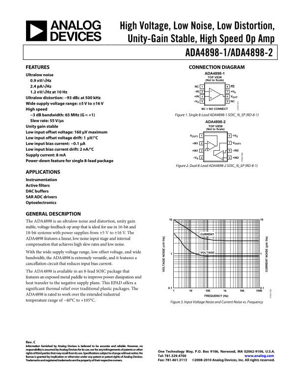
Page 1 Text Content
High Voltage, Low Noise, Low Distortion, Unity-Gain Stable, High Speed Op Amp
ADA4898-1/ADA4898-2 FEATURES CONNECTION DIAGRAM
ADA4898-1
Ultralow noise
TOP VIEW 0.9 n V/√Hz (Not to Scale)
2.4 p A/√Hz NC PD8 1.2 n V/√Hz at 10 Hz –IN +VS7 +IN VOUT6
Ultralow distortion: −93 d Bc at 500 k Hz
–VS NC5
Wide supply voltage range: ±5 V to ±16 V
High speed NC = NO CONNECT
−3 d B bandwidth: 65 MHz (G = +1) Figure 1. Single 8-Lead ADA4898-1 SOIC_N_EP (RD-8-1)
Slew rate: 55 V/µs
ADA4898-2 Unity gain stable TOP VIEW (Not to Scale)
Low input offset voltage: 160 µV maximum
VOUT1 +VS8
Low input offset voltage drift: 1 μV/°C
–IN1 VOUT27
Low input bias current: −0.1 µA Low input bias current drift: 2 n A/°C –IN26
Supply current: 8 m A
–VS +IN25
Power-down feature for single 8-lead package
VO LT IS (n V/ √H z)
Figure 2. Dual 8-Lead ADA4898-2 SOIC_N_EP (RD-8-1)
APPLICATIONS Instrumentation Active filters DAC buffers SAR ADC drivers Optoelectronics
GENERAL DESCRIPTION The ADA4898 is an ultralow noise and distortion, unity gain stable, voltage feedback op amp that is ideal for use in 16-bit and 18-bit systems with power supplies from ±5 V to ±16 V. The
CURRENT
ADA4898 features a linear, low noise input stage and internal
compensation that achieves high slew rates and low noise. With the wide supply voltage range, low offset voltage, and wide VOLTAGE bandwidth, the ADA4898 is extremely versatile, and it features a cancellation circuit that reduces input bias current.
EN IS (p /√ z)
The ADA4898 is available in an 8-lead SOIC package that features an exposed metal paddle to improve power dissipation and heat transfer to the negative supply plane. This EPAD offers a
significant thermal relief over traditional plastic packages. The 0.1 0.1
ADA4898 is rated to work over the extended industrial
FREQUENCY (Hz)
temperature range of −40°C to +105°C.
Figure 3. Input Voltage Noise and Current Noise vs. Frequency
Rev. C Information furnished by Analog Devices is believed to be accurate and reliable. However, no responsibility is assumed by Analog Devices for its use, nor for any infringements of patents or other
One Technology Way, P.O. Box 9106, Norwood, MA 02062-9106, U.S.A.
rights of third parties that may result from its use. Specifications subject to change without notice. No
license is granted by implication or otherwise under any patent or patent rights of Analog Devices. Tel: 781.329.4700 www.analog.com Trademarks and registered trademarks are the property of their respective owners. Fax: 781.461.3113 ©2008-2010 Analog Devices, Inc. All rights reserved.
Page Summary Contents For ANALOG DEVICES ADA4898-1 Data Sheet
Manual Details
| Brand | Analog Devices |
|---|---|
| Pages | 20 |
| File Size | 343.05 KB |
| Published | June 16, 2026 |
Enter the captcha to get the download link:

Frequently Asked Questions
What is the recommended method for dissipating heat for proper operation?
The 8-lead SOIC package features an exposed metal paddle (EPAD) to improve power dissipation and heat transfer to the negative supply plane.
What is the full operational temperature range of the ADA4898 op amp?
The device is rated to work over an extended industrial temperature range of -40°C to +105°C.
What key performance benefits define this high-speed amplifier?
It offers ultralow noise, ultralow distortion (-93 dBc at 500 kHz), and wide bandwidth (65 MHz).
What specific types of circuit applications is the ADA4898 suited for?
Recommended applications include instrumentation, active filters, DAC buffers, SAR ADC drivers, and optoelectronics.