ANALOG DEVICES ADA4899-1 Data Sheet User Guide
Summary
The ADA4899-1 is a high-performance, unity-gain stable operational amplifier engineered for demanding signal processing applications. Featuring ultralow noise (1 nV/√Hz) and exceptional bandwidth up to 600 MHz, this device excels in data acquisition, instrumentation, and communications electronics. The accompanying manual offers comprehensive guidance, detailing connection diagrams, detailed pinout information, and technical specifications required for optimal integration into systems like filters, ADC drivers, and baseband amplifiers.
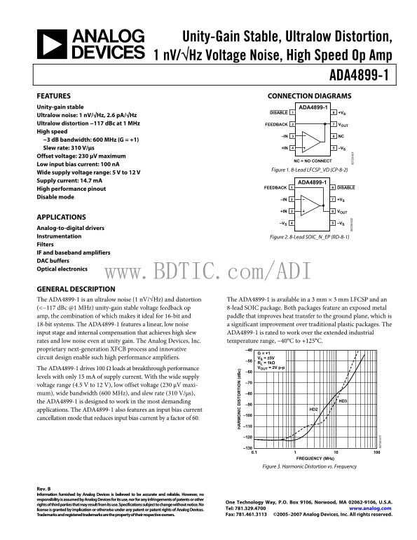
Page 1 Text Content
Unity-Gain Stable, Ultralow Distortion, 1 n V/√Hz Voltage Noise, High Speed Op Amp
ADA4899-1 FEATURES CONNECTION DIAGRAMS Unity-gain stable ADA4899-1
1DISABLE +VS8
Ultralow noise: 1 n V/√Hz, 2.6 p A/√Hz Ultralow distortion −117 d Bc at 1 MHz 2FEEDBACK VOUT7 High speed
3–IN NC6
−3 d B bandwidth: 600 MHz (G = +1)
Slew rate: 310 V/μs +IN –VS5
Offset voltage: 230 μV maximum
NC = NO CONNECT
Low input bias current: 100 n A
Figure 1. 8-Lead LFCSP_VD (CP-8-2)
Wide supply voltage range: 5 V to 12 V Supply current: 14.7 m A
ADA4899-1 1FEEDBACK DISABLE8
High performance pinout Disable mode
2–IN +VS7
3+IN VOUT6
APPLICATIONS
–VS –VS5
Analog-to-digital drivers Instrumentation Figure 2. 8-Lead SOIC_N_EP (RD-8-1)
IC IS TO TI (d c)
Filters IF and baseband amplifiers DAC buffers Optical electronics
www.BDTIC.com/ADI GENERAL DESCRIPTION The ADA4899-1 is an ultralow noise (1 n V/√Hz) and distortion The ADA4899-1 is available in a 3 mm × 3 mm LFCSP and an
(<−117 d Bc @1 MHz) unity-gain stable voltage feedback op 8-lead SOIC package. Both packages feature an exposed metal amp, the combination of which makes it ideal for 16-bit and paddle that improves heat transfer to the ground plane, which is 18-bit systems. The ADA4899-1 features a linear, low noise a significant improvement over traditional plastic packages. The input stage and internal compensation that achieves high slew ADA4899-1 is rated to work over the extended industrial
rates and low noise even at unity gain. The Analog Devices, Inc. temperature range, −40°C to +125°C.
proprietary next-generation XFCB process and innovative –40
circuit design enable such high performance amplifiers. VS = ±5V
–50 RL = 1kΩ The ADA4899-1 drives 100 Ω loads at breakthrough performance VOUT = 2V p-p –60
levels with only 15 m A of supply current. With the wide supply
voltage range (4.5 V to 12 V), low offset voltage (230 μV maxi-
mum), wide bandwidth (600 MHz), and slew rate (310 V/μs), –80
the ADA4899-1 is designed to work in the most demanding HD3
applications. The ADA4899-1 also features an input bias current HD2
cancellation mode that reduces input bias current by a factor of 60.
FREQUENCY (MHz)
Figure 3. Harmonic Distortion vs. Frequency
Rev. B Information furnished by Analog Devices is believed to be accurate and reliable. However, no responsibility is assumed by Analog Devices for its use, nor for any infringements of patents or other
One Technology Way, P.O. Box 9106, Norwood, MA 02062-9106, U.S.A.
rights of third parties that may result from its use. Specifications subject to change without notice. No
license is granted by implication or otherwise under any patent or patent rights of Analog Devices. Tel: 781.329.4700 www.analog.com Trademarks and registered trademarks are the property of their respective owners. Fax: 781.461.3113 ©2005–2007 Analog Devices, Inc. All rights reserved.
Page Summary Contents For ANALOG DEVICES ADA4899-1 Data Sheet User Guide
Manual Details
| Brand | Analog Devices |
|---|---|
| Pages | 20 |
| File Size | 627.83 KB |
| Published | June 15, 2026 |
Enter the captcha to get the download link:

Frequently Asked Questions
What is the ADA4899-1 suitable for?
It is ideal for high-performance applications like ADCs, filters, instrumentation amplifiers, and optical electronics.
How does the device handle heat in high-density systems?
The exposed metal pad improves heat transfer to the ground plane, making it suitable for 16-bit and 18-bit systems.
What is the temperature operating range of this amplifier?
The ADA4899-1 is rated to work over an extended industrial temperature range of -40°C to +125°C.
How can I improve measurement accuracy for low input currents?
A proprietary cancellation mode can reduce the input bias current by a factor of 60.