ANALOG DEVICES AD1376 AD1377 Data Sheet User Guide
Summary
These 16-bit ADCs are high-resolution analog-to-digital converters engineered for precision measurement, featuring internal references and fast conversion times with exceptional linearity. The manual provides comprehensive technical details covering operation modes, clock rate management, gain adjustment, and optimal signal handling. Designed for demanding environments requiring extreme accuracy and stability, they are ideal for applications such as medical/analytic instrumentation, industrial robotics, ATE systems, or sophisticated data acquisition platforms.
Page 1 Text Content
Complete, High Speed 16-Bit A/D Converters
AD1376/AD1377
FEATURES Digital output data is provided in parallel form with corresponding clock and status outputs. All digital inputs and
Complete 16-bit converters with reference and clock
outputs are TTL-compatible.
±0.003% maximum nonlinearity No missing codes to 14 bits over temperature
For the AD1376, the serial output function is no longer
Fast conversion
available after date code 0111. For the AD1377, the serial output
17 µs to 16 bits (AD1376)
function is no longer available after date code 0210. The option
10 µs to 16 bits (AD1377)
of applying an external clock on the CONVERT START pin to
Short cycle capability
slow down the internally set conversion time is no longer
Adjustable clock rate
supported for either part.
Parallel outputs Low power PRODUCT HIGHLIGHTS 645 m W typical (AD1376)
585 m W typical (AD1377) 1. The AD1376/AD1377 provide 16-bit resolution with a Industry-standard pinout maximum linearity error of ±0.003% (1/2 LSB14) at 25°C. GENERAL DESCRIPTION 2. The AD1376 conversion time is 14 µs (typical) short cycled to 14 bits, and 16 µs to 16 bits.
The AD1376/AD1377 are high resolution, 16-bit analog-to-
digital converters with internal reference, clock, and laser- 3. The AD1377 conversion time is 8 µs (typical) short cycled trimmed thin-film applications resistors. The AD1376/AD1377 to 14 bits, and 9 µs to 16 bits.
-B IT
are excellent for use in high resolution applications requiring
4. Two binary codes are available on the digital output. They
moderate speed and high accuracy or stability over commercial
are CSB (complementary straight binary) for unipolar input
temperature ranges (0°C to 70°C). They are packaged in
voltage ranges and COB (complementary offset binary) for
compact 32-lead, ceramic seam-sealed (hermetic), dual in-line
bipolar input ranges. Complementary twos complement
packages (DIP). Thin-film scaling resistors provide bipolar
(CTC) coding may be obtained by inverting Pin 1 (MSB).
input ranges of ±2.5 V, ±5 V, and ±10 V and unipolar input
5. The AD1376/AD1377 include internal reference and clock
ranges of 0 V to +5 V, 0 V to +10 V, and 0 V to +20 V.
with external clock rate adjust pin, and parallel digital outputs.
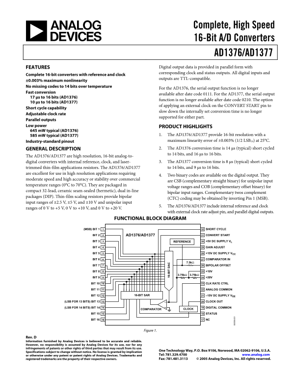
FUNCTIONAL BLOCK DIAGRAM
(MSB) BIT 1 SHORT CYCLE32
9- BIT 2 CONVERT START31
AD1376/AD1377
BIT 3 REFERENCE +5V DC SUPPLY VL30
BIT 4 GAIN ADJUST29
BIT 5 +15V DC SUPPLY VCC28
BIT 6 COMPARATOR IN27
BIT 7 BIPOLAR OFFSET26
BIT 8 +10V25
BIT 9 +20V24
BIT 10 CLK RATE CTRL23
BIT 11 ANALOG COMMON22
BIT 12 16-BIT SAR –15V DC SUPPLY VEE21
(LSB FOR 13 BITS) BIT 13 CLOCK OUT20
(LSB FOR 14 BITS) BIT 14 DIGITAL COMMON19
COMPARATOR CLOCK
BIT 15 STATUS18
BIT 16 NC17
Figure 1.
Rev. D Information furnished by Analog Devices is believed to be accurate and reliable. However, no responsibility is assumed by Analog Devices for its use, nor for any infringements of patents or other rights of third parties that may result from its use.
One Technology Way, P.O. Box 9106, Norwood, MA 02062-9106, U.S.A.
Specifications subject to change without notice. No license is granted by implication
or otherwise under any patent or patent rights of Analog Devices. Trademarks and Tel: 781.329.4700 www.analog.com registered trademarks are the property of their respective owners. Fax: 781.481.3113 © 2005 Analog Devices, Inc. All rights reserved.
Page Summary Contents For ANALOG DEVICES AD1376 AD1377 Data Sheet User Guide
Manual Details
| Brand | Analog Devices |
|---|---|
| Pages | 12 |
| File Size | 397.00 KB |
| Published | June 16, 2026 |
Enter the captcha to get the download link:

Frequently Asked Questions
What is the maximum linearity error for these converters?
The maximum nonlinearity error is ±0.003% (1/2 LSB14).
Can I use these AD1376/AD1377 converters in extreme temperatures?
No, they are specified for operation over commercial temperature ranges of 0°C to 70°C.
How fast can the AD1377 convert data?
The typical conversion time for the AD1377 is 8 µs (short cycled) to 16 bits.
What are some suitable applications for these high-resolution converters?
They are excellent for medical instrumentation, industrial robotics, ATE, and multichannel data acquisition systems.