ANALOG DEVICES AD8317 Product Data Sheet
Summary
The AD8317 is a high-performance demodulating logarithmic amplifier designed to accurately convert RF input signals (1 MHz to 10 GHz) into a linear voltage proportional to the signal's magnitude in decibels. This manual provides comprehensive coverage of its functionality, detailing both measurement mode for monitoring and advanced controller mode for closed-loop power regulation. Ideal for engineers developing RF communication systems, including base stations and transmitters, requiring precise level detection or power setpoint control.
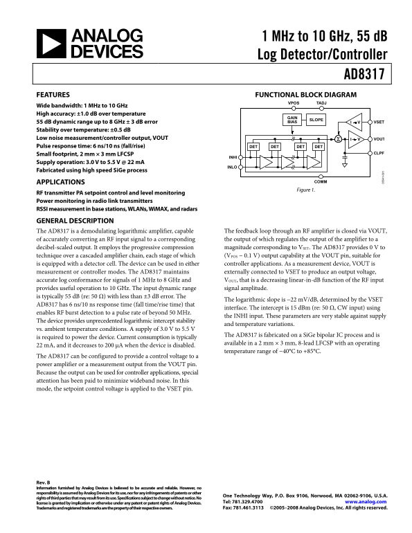
Page 1 Text Content
1 MHz to 10 GHz, 55 d B Log Detector/Controller
AD8317 FEATURES FUNCTIONAL BLOCK DIAGRAM
TADJVPOS
Wide bandwidth: 1 MHz to 10 GHz High accuracy: ±1.0 d B over temperature
SLOPE
55 d B dynamic range up to 8 GHz ± 3 d B error BIAS VSET
Stability over temperature: ±0.5 d B Low noise measurement/controller output, VOUT VOUT Pulse response time: 6 ns/10 ns (fall/rise) DET DET DET DET
Small footprint, 2 mm × 3 mm LFCSP CLPF
Supply operation: 3.0 V to 5.5 V @ 22 m A
Fabricated using high speed Si Ge process
APPLICATIONS COMM Figure 1.
RF transmitter PA setpoint control and level monitoring Power monitoring in radio link transmitters RSSI measurement in base stations, WLANs, Wi MAX, and radars
GENERAL DESCRIPTION
The AD8317 is a demodulating logarithmic amplifier, capable The feedback loop through an RF amplifier is closed via VOUT, of accurately converting an RF input signal to a corresponding the output of which regulates the output of the amplifier to a decibel-scaled output. It employs the progressive compression magnitude corresponding to VSET. The AD8317 provides 0 V to
technique over a cascaded amplifier chain, each stage of which (VPOS − 0.1 V) output capability at the VOUT pin, suitable for is equipped with a detector cell. The device can be used in either controller applications. As a measurement device, VOUT is measurement or controller modes. The AD8317 maintains externally connected to VSET to produce an output voltage, accurate log conformance for signals of 1 MHz to 8 GHz and VOUT, that is a decreasing linear-in-d B function of the RF input
provides useful operation to 10 GHz. The input dynamic range signal amplitude.
is typically 55 d B (re: 50 Ω) with less than ±3 d B error. The
The logarithmic slope is −22 m V/d B, determined by the VSET
AD8317 has 6 ns/10 ns response time (fall time/rise time) that
interface. The intercept is 15 d Bm (re: 50 Ω, CW input) using
enables RF burst detection to a pulse rate of beyond 50 MHz.
the INHI input. These parameters are very stable against supply
The device provides unprecedented logarithmic intercept stability
and temperature variations.
vs. ambient temperature conditions. A supply of 3.0 V to 5.5 V
The AD8317 is fabricated on a Si Ge bipolar IC process and is
is required to power the device. Current consumption is typically
available in a 2 mm × 3 mm, 8-lead LFCSP with an operating
22 m A, and it decreases to 200 μA when the device is disabled.
temperature range of −40°C to +85°C.
The AD8317 can be configured to provide a control voltage to a power amplifier or a measurement output from the VOUT pin. Because the output can be used for controller applications, special attention has been paid to minimize wideband noise. In this 1- mode, the setpoint control voltage is applied to the VSET pin.
Rev. B Information furnished by Analog Devices is believed to be accurate and reliable. However, no responsibility is assumed by Analog Devices for its use, nor for any infringements of patents or other
One Technology Way, P.O. Box 9106, Norwood, MA 02062-9106, U.S.A.
rights of third parties that may result from its use. Specifications subject to change without notice. No
license is granted by implication or otherwise under any patent or patent rights of Analog Devices. Tel: 781.329.4700 www.analog.com Trademarks and registered trademarks are the property of their respective owners. Fax: 781.461.3113 ©2005–2008 Analog Devices, Inc. All rights reserved.
Page Summary Contents For ANALOG DEVICES AD8317 Product Data Sheet
Manual Details
| Brand | Analog Devices |
|---|---|
| Pages | 20 |
| File Size | 775.17 KB |
| Published | June 15, 2026 |
Enter the captcha to get the download link:

Frequently Asked Questions
What is the operating temperature range for the AD8317?
It operates in a temperature range of -40°C to +85°C.
How is the AD8317 used as a controller?
In controller mode, VOUT controls the gain of a VGA or VVA with a positive gain sense (increasing voltage increases gain).
What frequencies does the AD8317 support?
It supports a wide bandwidth from 1 MHz to 10 GHz.
What is the typical input dynamic range and slope?
The input dynamic range is typically 55 dB, with a logarithmic slope of -22 mV/dB.