# A B C D E F G H I J K L M N O P Q R S T U V W X Y Z

ANALOG DEVICES ADG5208 Product Data Sheet Rev A

Summary

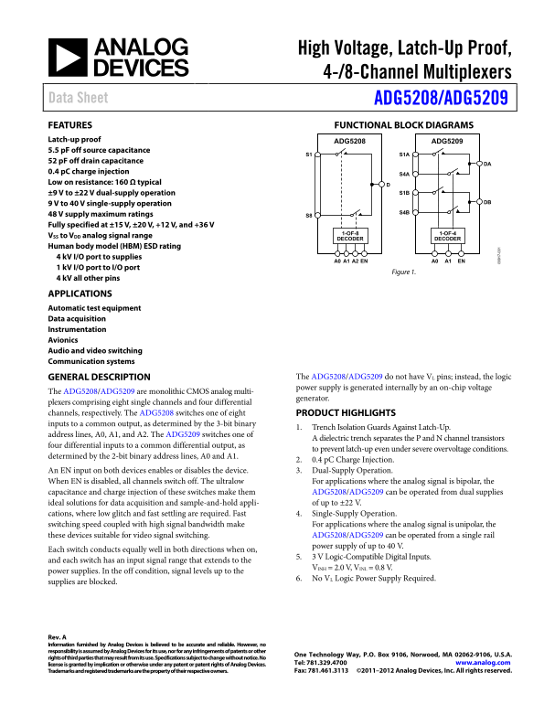
These advanced ADG5208/ADG5209 multiplexers are high-voltage, latch-up proof CMOS analog switches featuring both single and dual supply operation flexibility (up to ±22V or 40V). Built for demanding environments, the device efficiently switches large signal ranges with minimal charge injection. The manual provides comprehensive technical details on functional block diagrams, absolute maximum ratings, and performance characteristics. It is ideal for engineers utilizing data acquisition, instrumentation, avionics, and communication systems where reliable high-precision analog switching is required.
📄 Preview 📖 Table of Contents Contents PAGE OF 24

Page 1 Text Content

High Voltage, Latch-Up Proof, 4-/8-Channel Multiplexers

Data Sheet ADG5208/ADG5209 FEATURES FUNCTIONAL BLOCK DIAGRAMS Latch-up proof ADG5208 ADG5209 5.5 p F off source capacitance

52 p F off drain capacitance

0.4 p C charge injection

Low on resistance: 160 Ω typical

±9 V to ±22 V dual-supply operation S1B

9 V to 40 V single-supply operation DB

48 V supply maximum ratings S8 Fully specified at ±15 V, ±20 V, +12 V, and +36 V

1-OF-8 1-OF-4

VSS to VDD analog signal range

DECODER DECODER

Human body model (HBM) ESD rating 4 k V I/O port to supplies

A0 A1 A2 EN A0 A1 EN

1 k V I/O port to I/O port

Figure 1.

4 k V all other pins

APPLICATIONS Automatic test equipment Data acquisition Instrumentation Avionics Audio and video switching Communication systems

GENERAL DESCRIPTION The ADG5208/ADG5209 do not have VL pins; instead, the logic power supply is generated internally by an on-chip voltage

The ADG5208/ADG5209 are monolithic CMOS analog multi-

generator.

plexers comprising eight single channels and four differential channels, respectively. The ADG5208 switches one of eight PRODUCT HIGHLIGHTS inputs to a common output, as determined by the 3-bit binary

1. Trench Isolation Guards Against Latch-Up.

address lines, A0, A1, and A2. The ADG5209 switches one of

A dielectric trench separates the P and N channel transistors

four differential inputs to a common differential output, as

to prevent latch-up even under severe overvoltage conditions.

determined by the 2-bit binary address lines, A0 and A1.

2. 0.4 p C Charge Injection.

An EN input on both devices enables or disables the device. 3. Dual-Supply Operation. When EN is disabled, all channels switch off. The ultralow For applications where the analog signal is bipolar, the capacitance and charge injection of these switches make them ADG5208/ADG5209 can be operated from dual supplies

ideal solutions for data acquisition and sample-and-hold appli- of up to ±22 V. cations, where low glitch and fast settling are required. Fast 4. Single-Supply Operation. switching speed coupled with high signal bandwidth make For applications where the analog signal is unipolar, the these devices suitable for video signal switching. ADG5208/ADG5209 can be operated from a single rail

power supply of up to 40 V.

Each switch conducts equally well in both directions when on,

5. 3 V Logic-Compatible Digital Inputs.

and each switch has an input signal range that extends to the

VINH = 2.0 V, VINL = 0.8 V.

power supplies. In the off condition, signal levels up to the

6. No VL Logic Power Supply Required.

supplies are blocked.

Rev. A Information furnished by Analog Devices is believed to be accurate and reliable. However, no responsibility is assumed by Analog Devices for its use, nor for any infringements of patents or other

One Technology Way, P.O. Box 9106, Norwood, MA 02062-9106, U.S.A.

rights of third parties that may result from its use. Specifications subject to change without notice. No

license is granted by implication or otherwise under any patent or patent rights of Analog Devices. Tel: 781.329.4700 www.analog.com Trademarks and registered trademarks are the property of their respective owners. Fax: 781.461.3113 ©2011–2012 Analog Devices, Inc. All rights reserved.

Page Summary Contents For ANALOG DEVICES ADG5208 Product Data Sheet Rev A

Page 1 High Voltage, Latch-Up Proof, 4-/8-Channel Multiplexers Data Sheet ADG5208/ADG5209 FEATURES FUNCTIONAL BLOCK DIAGRAMS Latch-up proof ADG5208 ADG5209 5.5 p F off source capacitance 52 p F off drain cap...
Page 2 ADG5208/ADG5209 Data Sheet TABLE OF CONTENTS Features .............................................................................................. 1 Absolute Maximum Ratings ...........................
Page 3 Data Sheet ADG5208/ADG5209 SPECIFICATIONS ±15 V DUAL SUPPLY VDD = +15 V ± 10%, VSS = −15 V ± 10%, GND = 0 V, unless otherwise noted. Table 1. Parameter 25°C −40°C to +85°C −40°C to +125°C Unit Test Co...
Page 4 ADG5208/ADG5209 Data Sheet Parameter 25°C −40°C to +85°C −40°C to +125°C Unit Test Conditions/Comments CD (On), CS (On) ADG5208 58 p F typ VS = 0 V, f = 1 MHz ADG5209 31 p F typ VS = 0 V, f = 1 MHz PO...
Page 5 Data Sheet ADG5208/ADG5209 Parameter 25°C −40°C to +85°C −40°C to +125°C Unit Test Conditions/Comments −3 d B Bandwidth RL = 50 Ω, CL = 5 p F; see Figure 32 ADG5208 60 MHz typ ADG5209 130 MHz typ Inse...
Page 6 ADG5208/ADG5209 Data Sheet Parameter 25°C −40°C to +85°C −40°C to +125°C Unit Test Conditions/Comments DYNAMIC CHARACTERISTICS1 Transition Time, t TRANSITION 210 ns typ RL = 300 Ω, CL = 35 p F 270 330...
Page 7 Data Sheet ADG5208/ADG5209 Parameter 25°C −40°C to +85°C −40°C to +125°C Unit Test Conditions/Comments Drain Off Leakage, ID (Off ) ±0.005 n A typ VS = 1 V/30 V, VD = 30 V/1 V; see Figure 30 ±0.1 ±0.4...
Page 8 ADG5208/ADG5209 Data Sheet CONTINUOUS CURRENT PER CHANNEL, Sx, D, OR Dx Table 5. ADG5208 Parameter 25°C 85°C 125°C Unit CONTINUOUS CURRENT, Sx OR D VDD = +15 V, VSS = −15 V TSSOP (θJA = 112.6°C/W) 40 ...
Page 9 Data Sheet ADG5208/ADG5209 ABSOLUTE MAXIMUM RATINGS TA = 25°C, unless otherwise noted. Stresses above those listed under Absolute Maximum Ratings Table 7. may cause permanent damage to the device. Thi...
Page 10 ADG5208/ADG5209 Data Sheet PIN CONFIGURATIONS AND FUNCTION DESCRIPTIONS EN A215 VSS GND14 ADG5208 VSS GND S1 TOP VIEW VDD13 (Not to Scale) 2S1 ADG5208 VDD TOP VIEW S3 S611 (Not to Scale) NOTES 1. THE ...
Page 11 Data Sheet ADG5208/ADG5209 EN GND15 VSS VDD14 ADG5209 S1A S1B13 VSS VDD TOP VIEW (Not to Scale) S2A S2B12 2S1A ADG5209 S1B S3A S3B11 TOP VIEW (Not to Scale) DA DB9 NOTES 1. THE EXPOSED PAD IS CONNECTE...
Page 12 ADG5208/ADG5209 Data Sheet ES IS TA (Ω ES IS TA (Ω ES IS TA (Ω TYPICAL PERFORMANCE CHARACTERISTICS TA = 25°C TA = 25°C VDD = 32.4V VDD = +18V VSS = 0V VSS = –18V VDD = 39.6V VDD = 36V VDD = +20V VSS =...
Page 13 Data Sheet ADG5208/ADG5209 LE EN (p ES IS TA (Ω ES IS TA (Ω IS (OFF) + – ID (OFF) + – ID (OFF) – + TA = +125°C TA = +85°C IS (OFF) – + TA = +25°C TA = –40°C –100 ID, IS (ON) + + ID, IS (ON) – – VDD = ...
Page 14 ADG5208/ADG5209 Data Sheet IN JE TI (p SS TA LK (d FF IS LA TI (d TA = 25°C TA = 25°C VDD = +15V VDD = +15V –20 VSS = –15V VSS = –15V –20 NO DECOUPLING –60 CAPACITORS DECOUPLING CAPACITORS FREQUENCY (...
Page 15 Data Sheet ADG5208/ADG5209 PA IT (p F) TI (n s) TA = 25°C VDD = +15V VSS = –15V VDD = +12V SOURCE/DRAIN ON VDD = +36V VSS = 0V VSS = 0V DRAIN OFF VDD = +15V VDD = +20V VSS = –15V VSS = –20V SOURCE OFF...
Page 16 ADG5208/ADG5209 Data Sheet TEST CIRCUITS ID (ON) IS (OFF) ID (OFF) Sx Sx DA VD VS VD NC = NO CONNECT Figure 27. On Leakage Figure 30. Off Leakage VDD VSS 0.1µF 0.1µF NETWORK 7- ANALYZER VDD VSS V1 RL ...
Page 17 Data Sheet ADG5208/ADG5209 VDD VSS 3V tr < 20ns tf < 20ns VDD VSS ADDRESS DRIVE (VIN) A0 S1 VS1 S2 TO S7 t TRANSITION t TRANSITION S8 VS8 OUTPUTADG5208* 2.0V EN OUTPUT 300ΩGND 35p F *SIMILAR CON...
Page 18 ADG5208/ADG5209 Data Sheet VDD VSS VDD VSS ADG5208* RS DS VOUT VOUT ΔVOUT QINJ = CL × ΔVOUT VS GND *SIMILAR CONNECTION FOR ADG5209. Figure 36. Charge Injection Rev. A | Page 18 of 24
Page 19 Data Sheet ADG5208/ADG5209 TERMINOLOGY IDD CIN IDD represents the positive supply current. CIN represents digital input capacitance. ISS t ON (EN) ISS represents the negative supply current. t ON (EN)...
Page 20 ADG5208/ADG5209 Data Sheet TRENCH ISOLATION NMOS PMOS In the ADG5208/ADG5209, an insulating oxide layer (trench) is placed between the NMOS and the PMOS transistors of each CMOS switch. Parasitic junc...
Page 21 Data Sheet ADG5208/ADG5209 APPLICATIONS INFORMATION The ADG52xx family of switches and multiplexers provides a robust solution for instrumentation, industrial, automotive, aerospace, and other harsh e...
Page 22 ADG5208/ADG5209 Data Sheet OUTLINE DIMENSIONS 4.40 BSC 4.30 PIN 1 1.20 MAX 0.19 SEATING PLANE COPLANARITY 0.10 COMPLIANT TO JEDEC STANDARDS MO-153-AB Figure 38. 16-Lead Thin Shrink Small Outline Packa...
Page 23 Data Sheet ADG5208/ADG5209 NOTES Rev. A | Page 23 of 24
Page 24 ADG5208/ADG5209 Data Sheet NOTES ©2011–2012 Analog Devices, Inc. All rights reserved. Trademarks and registered trademarks are the property of their respective owners. D09917-0-3/12(A) Rev. A | Page 2...