ANALOG DEVICES ADG5204 Product Data Handbook Rev 0
Summary
The ADG5204 is a high voltage, latch-up proof 4-channel analog multiplexer designed for demanding instrumentation environments. Featuring trench isolation, it ensures reliable signal switching even under severe overvoltage conditions. It offers flexible operation via both single (up to 40V) and dual power supplies (up to ±22V), boasts ultralow capacitance, and utilizes a break-before-make switching action. It is the perfect solution for automated test equipment, data acquisition systems, avionics, and advanced communication applications requiring high performance and robust signal integrity.
Page 1 Text Content
High Voltage, Latch-Up Proof, 4-Channel Multiplexer
ADG5204 FEATURES FUNCTIONAL BLOCK DIAGRAM Latch-up proof ADG5204 3 p F off source capacitance
26 p F off drain capacitance
−0.6 p C charge injection
Low leakage: 0.4 n A maximum at 85°C
±9 V to ±22 V dual-supply operation
1 OF 4 9 V to 40 V single-supply operation DECODERS
48 V supply maximum ratings
A0 A1 EN
Fully specified at ±15 V, ±20 V, +12 V, and +36 V
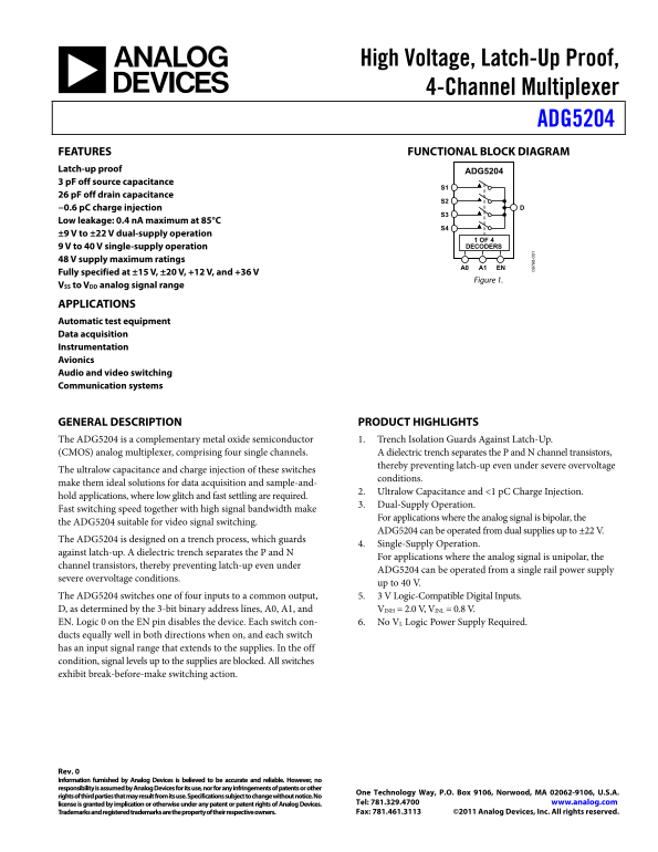
Figure 1.
VSS to VDD analog signal range
APPLICATIONS Automatic test equipment Data acquisition Instrumentation Avionics Audio and video switching Communication systems
GENERAL DESCRIPTION PRODUCT HIGHLIGHTS The ADG5204 is a complementary metal oxide semiconductor 1. Trench Isolation Guards Against Latch-Up. (CMOS) analog multiplexer, comprising four single channels. A dielectric trench separates the P and N channel transistors,
thereby preventing latch-up even under severe overvoltage
The ultralow capacitance and charge injection of these switches
conditions.
make them ideal solutions for data acquisition and sample-and-
2. Ultralow Capacitance and <1 p C Charge Injection.
hold applications, where low glitch and fast settling are required.
3. Dual-Supply Operation.
Fast switching speed together with high signal bandwidth make
For applications where the analog signal is bipolar, the
the ADG5204 suitable for video signal switching.
ADG5204 can be operated from dual supplies up to ±22 V. 8-
The ADG5204 is designed on a trench process, which guards
4. Single-Supply Operation.
against latch-up. A dielectric trench separates the P and N
For applications where the analog signal is unipolar, the
channel transistors, thereby preventing latch-up even under
ADG5204 can be operated from a single rail power supply
severe overvoltage conditions.
up to 40 V.
The ADG5204 switches one of four inputs to a common output, 5. 3 V Logic-Compatible Digital Inputs. D, as determined by the 3-bit binary address lines, A0, A1, and VINH = 2.0 V, VINL = 0.8 V. EN. Logic 0 on the EN pin disables the device. Each switch con- 6. No VL Logic Power Supply Required. ducts equally well in both directions when on, and each switch has an input signal range that extends to the supplies. In the off condition, signal levels up to the supplies are blocked. All switches exhibit break-before-make switching action.
Rev. 0 Information furnished by Analog Devices is believed to be accurate and reliable. However, no responsibility is assumed by Analog Devices for its use, nor for any infringements of patents or other
One Technology Way, P.O. Box 9106, Norwood, MA 02062-9106, U.S.A.
rights of third parties that may result from its use. Specifications subject to change without notice. No
license is granted by implication or otherwise under any patent or patent rights of Analog Devices. Tel: 781.329.4700 www.analog.com Trademarks and registered trademarks are the property of their respective owners. Fax: 781.461.3113 ©2011 Analog Devices, Inc. All rights reserved.
Page Summary Contents For ANALOG DEVICES ADG5204 Product Data Handbook Rev 0
Manual Details
| Brand | Analog Devices |
|---|---|
| Pages | 20 |
| File Size | 334.84 KB |
| Published | June 15, 2026 |
Enter the captcha to get the download link:

Frequently Asked Questions
How does the ADG5204 prevent latch-up failure?
It includes a dielectric trench isolation process which separates the P and N channel transistors, guarding against latch-up even under severe overvoltage conditions.
What types of analog signals can the MUX handle?
It is suitable for bipolar signals (using dual supplies up to ±22 V) or unipolar signals (using single supply up to 40 V).
Is the device compatible with modern signal processing needs?
Yes, it features ultralow capacitance and charge injection, making it ideal for data acquisition and sample-and-hold applications requiring low glitch.
What is the switching mechanism like when operating the device?
All four switches exhibit a break-before-make switching action to ensure clean signal integrity during transitions.