AMD AM28F010 Memory User Manual - Supermicro Semiconductor
Summary
This 1 Megabit Flash memory offers highly reliable, non-volatile storage designed for demanding embedded systems requiring frequent reprogramming capability. It ensures robust data retention and operation with low power consumption while meeting strict JEDEC standards. This technical guide provides detailed specifications, usage protocols, and optimized programming algorithms (including command register architecture) necessary for seamless system design and integration by electrical engineers and hardware developers building high-performance, long-lasting electronics.
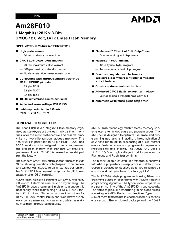
Page 1 Text Content
FINAL
Am28F010 1 Megabit (128 K x 8-Bit) CMOS 12.0 Volt, Bulk Erase Flash Memory DISTINCTIVE CHARACTERISTICS High performance Flasherase™ Electrical Bulk Chip-Erase 70 ns maximum access time One second typical chip-erase CMOS Low power consumption Flashrite™ Programming 30 m A maximum active current 10 µs typical byte-program 100 µA maximum standby current Two seconds typical chip program No data retention power consumption
Command register architecture for microprocessor/microcontroller compatible
Compatible with JEDEC-standard byte-wide
write interface
32-Pin EPROM pinouts
32-pin PDIP On-chip address and data latches
32-pin PLCC
Advanced CMOS flash memory technology
32-pin TSOP
Low cost single transistor memory cell
10,000 write/erase cycles minimum
Automatic write/erase pulse stop timer
Write and erase voltage 12.0 V ±5% Latch-up protected to 100 m A from –1 V to VCC +1 V
GENERAL DESCRIPTION The Am28F010 is a 1 Megabit Flash memory orga- AMD’s Flash technology reliably stores memory con- nized as 128 Kbytes of 8 bits each. AMD’s Flash mem- tents even after 10,000 erase and program cycles. The ories offer the most cost-effective and reliable read/ AMD cell is designed to optimize the erase and pro- write non-volati le random access memory. The gramming mechanisms. In addition, the combination of Am28F010 is packaged in 32-pin PDIP, PLCC, and advanced tunnel oxide processing and low internal TSOP versions. It is designed to be reprogrammed electric fields for erase and programming operations and erased in-system or in standard EPROM pro- produces reliable cycling. The Am28F010 uses a grammers. The Am28F010 is erased when shipped 12.0V 5% VPP high voltage input to perform the
from the factory. Flasherase and Flashrite algorithms. The standard Am28F010 offers access times as fast as The highest degree of latch-up protection is achieved 70 ns, allowing operation of high-speed microproces- with AMD’s proprietary non-epi process. Latch-up pro- sors without wait states. To eliminate bus contention, tection is provided for stresses up to 100 milliamps on the Am28F010 has separate chip enable (CE#) and address and data pins from –1 V to VCC +1 V.
output enable (OE#) controls.
The Am28F010 is byte programmable using 10 ms pro- AMD’s Flash memories augment EPROM functionality gramming pulses in accordance with AMD’s Flashrite with in-circuit electrical erasure and programming. The programming algorithm. The typical room temperature Am28F010 uses a command register to manage this programming time of the Am28F010 is two seconds. functionality, while maintaining a JEDEC Flash Stan- The entire chip is bulk erased using 10 ms erase pulses dard 32-pin pinout. The command register allows for according to AMD’s Flasherase alrogithm. Typical era- 100% TTL level control inputs and fixed power supply sure at room temperature is accomplished in less than levels during erase and programming, while maintain- one second. The windowed package and the 15–20
ing maximum EPROM compatibility.
Publication# 11559 Rev: H Amendment/+2 Issue Date: January 1998
Page Summary Contents For AMD AM28F010 Memory User Manual - Supermicro Semiconductor
Manual Details
| Brand | AMD |
|---|---|
| Pages | 36 |
| File Size | 466.83 KB |
| Published | May 14, 2026 |
Enter the captcha to get the download link:

Frequently Asked Questions
What is the memory capacity and organization of the Am28F010?
It is a 1 Megabit Flash memory, organized as 128 Kbytes of 8 bits each.
How long does it take to erase or program the memory chip?
The typical chip-erase time is one second, and the typical chip program time is two seconds.
Does the device have protection against electrical surges?
Yes, it is latch-up protected up to 100 mA from –1 V to V +1 V.
How many write/erase cycles can the Am28F010 endure?
It guarantees a minimum of 10,000 write/erase cycles.