AMD DS42553 Handbook
Summary
This technical manual provides comprehensive information on the DS42553 MCP device, a high-performance 32Mbit Flash Memory and 4 Mbit SRAM solution designed for advanced embedded systems. It details architectural improvements such as zero-latency read/write operations and Secured Silicon (SecSi) technology for secure data management. The guide covers hardware features, performance specifications, power consumption profiles, and software methods using the Data Management Software (DMS). Ideal for system engineers designing low-power, high-reliability devices that require non-volatile, protected storage capabilities.
Page 1 Text Content
查询DS42553供应商
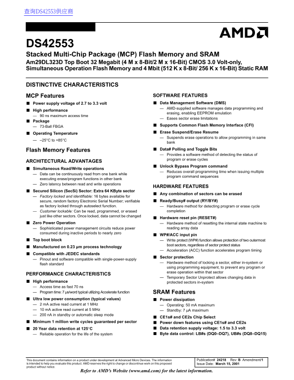
DS42553 Stacked Multi-Chip Package (MCP) Flash Memory and SRAM Am29DL323D Top Boot 32 Megabit (4 M x 8-Bit/2 M x 16-Bit) CMOS 3.0 Volt-only, Simultaneous Operation Flash Memory and 4 Mbit (512 K x 8-Bit/ 256 K x 16-Bit) Static RAM
DISTINCTIVE CHARACTERISTICS
MCP Features SOFTWARE FEATURES Power supply voltage of 2.7 to 3.3 volt Data Management Software (DMS) AMD-supplied software manages data programming and
High performance
erasing, enabling EEPROM emulation
90 ns maximum access time
Eases sector erase limitations
Package
Supports Common Flash Memory Interface (CFI)
73-Ball FBGA
Erase Suspend/Erase Resume
Operating Temperature
Suspends erase operations to allow programming in same
–25°C to +85°C
Flash Memory Features Data# Polling and Toggle Bits Provides a software method of detecting the status of program or erase cycles
ARCHITECTURAL ADVANTAGES
Unlock Bypass Program command
Simultaneous Read/Write operations
Reduces overall programming time when issuing multiple
Data can be continuously read from one bank while
program command sequences
executing erase/program functions in other bank Zero latency between read and write operations
HARDWARE FEATURES
Secured Silicon (Sec Si) Sector: Extra 64 KByte sector
Any combination of sectors can be erased
Factory locked and identifiable: 16 bytes available for
secure, random factory Electronic Serial Number; verifiable Ready/Busy# output (RY/BY#)
as factory locked through autoselect function. Hardware method for detecting program or erase cycle
Customer lockable: Can be read, programmed, or erased completion
just like other sectors. Once locked, data cannot be changed
Hardware reset pin (RESET#)
Zero Power Operation Hardware method of resetting the internal state machine to
Sophisticated power management circuits reduce power reading array data
consumed during inactive periods to nearly zero
WP#/ACC input pin
Top boot block Write protect (WP#) function allows protection of two outermost
boot sectors, regardless of sector protect status
Manufactured on 0.23 µm process technology
Acceleration (ACC) function accelerates program timing
Compatible with JEDEC standards
Sector protection
Pinout and software compatible with single-power-supply
Hardware method of locking a sector, either in-system or
flash standard
using programming equipment, to prevent any program or erase operation within that sector
PERFORMANCE CHARACTERISTICS
Temporary Sector Unprotect allows changing data in
High performance protected sectors in-system Access time as fast 70 ns Program time: 7 µs/word typical utilizing Accelerate function SRAM Features Ultra low power consumption (typical values) Power dissipation 2 m A active read current at 1 MHz Operating: 50 m A maximum 10 m A active read current at 5 MHz Standby: 7 µA maximum 200 n A in standby or automatic sleep mode
CE1s# and CE2s Chip Select
Minimum 1 million write cycles guaranteed per sector Power down features using CE1s# and CE2s
20 Year data retention at 125°C Data retention supply voltage: 1.5 to 3.3 volt Reliable operation for the life of the system Byte data control: LB#s (DQ0–DQ7), UB#s (DQ8–DQ15)
This document contains information on a product under development at Advanced Micro Devices. The information Publication# 24218 Rev: B Amendment/1
is intended to help you evaluate this product. AMD reserves the right to change or discontinue work on this proposed Issue Date: March 15, 2001 product without notice.
Refer to AMD’s Website (www.amd.com) for the latest information.
Page Summary Contents For AMD DS42553 Handbook
Manual Details
| Brand | AMD |
|---|---|
| Pages | 58 |
| File Size | 482.00 KB |
| Published | May 14, 2026 |
Enter the captcha to get the download link:

Frequently Asked Questions
How does this chip improve read/write performance?
By allowing simultaneous read/write operations, it reduces overall programming time and offers zero latency between read and write operations.
What security features are built into the memory?
It includes a Secured Silicon (SecSi) sector that can be factory locked or customer lockable to prevent any data changes.
Is this device compliant with industry standards?
Yes, it supports the Common Flash Memory Interface (CFI) and is pinout/software compatible with JEDEC standards.
What are its power consumption characteristics?
In standby mode, the maximum consumption is very low at 7 µA, making it reliable for long-life system operation.