AMD Am28F010 1 Megabit (128 K x 8-Bit) CMOS 12.0 Volt Bulk Erase Flash Memory User Manual
Summary
The Am28F010 is a high-performance 1 Megabit Flash memory semiconductor, perfect for embedding reliable, non-volatile random access data storage in demanding electronic systems. This guide provides comprehensive technical specifications, detailing advanced chip-erase/programming algorithms and low-power consumption features for ease of design integration. It is essential reading for electrical engineers and hardware developers requiring robust, fast-access memory solutions compatible with modern microprocessors and embedded control applications.
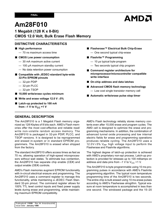
Page 1 Text Content
FINAL
Am28F010 1 Megabit (128 K x 8-Bit) CMOS 12.0 Volt, Bulk Erase Flash Memory DISTINCTIVE CHARACTERISTICS High performance Flasherase™ Electrical Bulk Chip-Erase 70 ns maximum access time One second typical chip-erase CMOS Low power consumption Flashrite™ Programming 30 m A maximum active current 10 µs typical byte-program 100 µA maximum standby current Two seconds typical chip program No data retention power consumption
Command register architecture for microprocessor/microcontroller compatible
Compatible with JEDEC-standard byte-wide
write interface
32-Pin EPROM pinouts
32-pin PDIP On-chip address and data latches
32-pin PLCC
Advanced CMOS flash memory technology
32-pin TSOP
Low cost single transistor memory cell
10,000 write/erase cycles minimum
Automatic write/erase pulse stop timer
Write and erase voltage 12.0 V ±5% Latch-up protected to 100 m A from –1 V to VCC +1 V
GENERAL DESCRIPTION The Am28F010 is a 1 Megabit Flash memory orga- AMD’s Flash technology reliably stores memory con- nized as 128 Kbytes of 8 bits each. AMD’s Flash mem- tents even after 10,000 erase and program cycles. The ories offer the most cost-effective and reliable read/ AMD cell is designed to optimize the erase and pro- write non-volati le random access memory. The gramming mechanisms. In addition, the combination of Am28F010 is packaged in 32-pin PDIP, PLCC, and advanced tunnel oxide processing and low internal TSOP versions. It is designed to be reprogrammed electric fields for erase and programming operations and erased in-system or in standard EPROM pro- produces reliable cycling. The Am28F010 uses a grammers. The Am28F010 is erased when shipped 12.0V 5% VPP high voltage input to perform the
from the factory. Flasherase and Flashrite algorithms. The standard Am28F010 offers access times as fast as The highest degree of latch-up protection is achieved 70 ns, allowing operation of high-speed microproces- with AMD’s proprietary non-epi process. Latch-up pro- sors without wait states. To eliminate bus contention, tection is provided for stresses up to 100 milliamps on the Am28F010 has separate chip enable (CE#) and address and data pins from –1 V to VCC +1 V.
output enable (OE#) controls.
The Am28F010 is byte programmable using 10 ms pro- AMD’s Flash memories augment EPROM functionality gramming pulses in accordance with AMD’s Flashrite with in-circuit electrical erasure and programming. The programming algorithm. The typical room temperature Am28F010 uses a command register to manage this programming time of the Am28F010 is two seconds. functionality, while maintaining a JEDEC Flash Stan- The entire chip is bulk erased using 10 ms erase pulses dard 32-pin pinout. The command register allows for according to AMD’s Flasherase alrogithm. Typical era- 100% TTL level control inputs and fixed power supply sure at room temperature is accomplished in less than levels during erase and programming, while maintain- one second. The windowed package and the 15–20
ing maximum EPROM compatibility.
Publication# 11559 Rev: H Amendment/+2 Issue Date: January 1998
Page Summary Contents For AMD Am28F010 1 Megabit (128 K x 8-Bit) CMOS 12.0 Volt Bulk Erase Flash Memory User Manual
Manual Details
| Brand | AMD |
|---|---|
| Pages | 35 |
| File Size | 464.38 KB |
| Published | May 14, 2026 |
Enter the captcha to get the download link:

Frequently Asked Questions
What is the minimum write/erase cycle life for this memory chip?
The Am28F010 offers a minimum of 10,000 write/erase cycles.
How does the device handle high electrical stress during operation?
It includes latch-up protection for stresses up to 100 mA from –1 V to V +1 V, and separate CE# and OE# controls are provided.
What is the fastest data access time available?
The fastest access time listed is 70 ns for all primary signal inputs (CE#, OE#) and the data bus.
Are there different physical packages available for this memory chip?
Yes, it comes in 32-pin PDIP, PLCC, or TSOP versions.