# A B C D E F G H I J K L M N O P Q R S T U V W X Y Z

AD8339 Rev. 0 Data Sheet - DC to 50 MHz, Quad IQ Demodulator and Phase Shifter

Summary

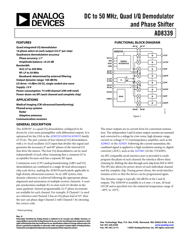
This quad I/Q demodulator and phase shifter is a high-performance RF component designed for complex signal processing by performing quadrature demodulation and enabling beamforming. It features four independent I/Q channels with 16 programmable phase steps for precise alignment, making it ideal for applications requiring channel summation, such as phased array systems, advanced radar units, and medical ultrasound imaging devices. The manual details its functional operation, electrical specifications, and implementation guidelines across various high-density communication receiver architectures.
📄 Preview 📖 Table of Contents Contents PAGE OF 36

Page 1 Text Content

DC to 50 MHz, Quad I/Q Demodulator

and Phase Shifter

AD8339 FEATURES FUNCTIONAL BLOCK DIAGRAM

RF1PRF1N

Quad integrated I/Q demodulator 16 phase select on each output (22.5° per step) AD8339 Quadrature demodulation accuracy I1OP

Phase accuracy: ±1° SCLK SDI SERIAL

Amplitude balance: ±0.25 d B Q1OP

SDO INTERFACE

Bandwidth CSB

4LO: LF to 200 MHz I2OP

RF: LF to 50 MHz RF2N

Baseband: determined by external filtering

Output dynamic range: 160 d B/Hz ÷4 90°

LO drive: >0 d Bm (50 Ω), single-ended sine wave

Supply: ±5 V RF3N

Power consumption: 73 m W/channel (290 m W total)

Power-down via SPI (each channel and complete chip)

BIAS I4OP

APPLICATIONS

Medical imaging (CW ultrasound beamforming) Phased array systems

RF4PRF4N

Radar Adaptive antennas

Figure 1.

Communication receivers

GENERAL DESCRIPTION The AD83391 is a quad I/Q demodulator configured to be The mixer outputs are in current form for convenient summa- driven by a low noise preamplifier with differential outputs. It is tion. The independent I and Q mixer output currents are summed optimized for the LNA in the AD8332/AD8334/AD8335 family and converted to a voltage by a low noise, high dynamic range,

of VGAs. The part consists of four identical I/Q demodulators current-to-voltage (I-V) transimpedance amplifier, such as the

with a 4× local oscillator (LO) input that divides this signal and AD8021 or the AD829. Following the current summation, the generates the necessary 0° and 90° phases of the internal LO combined signal is applied to a high resolution analog-to-digital

that drive the mixers. The four I/Q demodulators can be used converter (ADC), such as the AD7665 (16-bit, 570 k SPS).

independently of each other (assuming that a common LO is

An SPI-compatible serial interface port is provided to easily

acceptable) because each has a separate RF input.

program the phase of each channel; the interface allows daisy Continuous wave (CW) analog beamforming (ABF) and I/Q chaining by shifting the data through each chip from SDI to SDO.

demodulation are combined in a single 40-lead ultracompact The SPI also allows for power-down of each individual channel chip scale device, making the AD8339 particularly applicable in and the complete chip. During power-down, the serial interface high density ultrasound scanners. In an ABF system, time remains active so that the device can be programmed again.

domain coherency is achieved following the appropriate phase

The dynamic range is typically 160 d B/Hz at the I and Q

alignment and summation of multiple receiver channels. A reset

outputs. The AD8339 is available in a 6 mm × 6 mm, 40-lead

pin synchronizes multiple ICs to start each LO divider in the

LFCSP and is specified over the industrial temperature range of

same quadrant. Sixteen programmable 22.5° phase increments

−40°C to +85°C.

are available for each channel. For example, if Channel 1 is used as a reference and Channel 2 has an I/Q phase lead of 45°, then the user can phase align Channel 2 with Channel 1 by choosing the correct code.

1 Patent pending.

Rev. 0 Information furnished by Analog Devices is believed to be accurate and reliable. However, no responsibility is assumed by Analog Devices for its use, nor for any infringements of patents or other

One Technology Way, P.O. Box 9106, Norwood, MA 02062-9106, U.S.A.

rights of third parties that may result from its use. Specifications subject to change without notice. No

license is granted by implication or otherwise under any patent or patent rights of Analog Devices. Tel: 781.329.4700 www.analog.com Trademarks and registered trademarks are the property of their respective owners. Fax: 781.461.3113 ©2007 Analog Devices, Inc. All rights reserved.

Page Summary Contents For AD8339 Rev. 0 Data Sheet - DC to 50 MHz, Quad IQ Demodulator and Phase Shifter

Page 1 DC to 50 MHz, Quad I/Q Demodulator and Phase Shifter AD8339 FEATURES FUNCTIONAL BLOCK DIAGRAM RF1PRF1N Quad integrated I/Q demodulator 16 phase select on each output (22.5° per step) AD8339 Quadrature...
Page 2 AD8339 TABLE OF CONTENTS Features Summation of Multiple Channels (Analog Beamforming).. Applications....................................................................................... Phase Compen...
Page 3 AD8339 SPECIFICATIONS VS = ±5 V, TA = 25°C, 4f LO = 20 MHz, f RF = 5.01 MHz, f BB = 10 k Hz, PLO ≥ 0 d Bm, per channel performance, d Bm (50 Ω), unless otherwise noted. Single-channel AD8021 LPF value...
Page 4 AD8339 Parameter Conditions Min Typ Max Unit LOGIC INTERFACES Logic Level High Pin SDI, Pin CSB, Pin SCLK, Pin RSET 1.5 V Logic Level Low 0.9 V Logic Level High Pin RSTS 1.8 V Logic Level Low 1.2 V Bi...
Page 5 AD8339 ABSOLUTE MAXIMUM RATINGS Table 2. Stresses above those listed under Absolute Maximum Ratings Parameter Rating may cause permanent damage to the device. This is a stress Voltages rating only; fu...
Page 6 AD8339 PIN CONFIGURATION AND FUNCTION DESCRIPTIONS RF2N Q2OP RF2P 9PIN 1 I2OP COMM INDICATOR VPOS COMM VPOS SCLK AD8339 CSB 4LON (Not to Scale) VPOS VNEG VPOS VNEG RF3P I3OP RF3N Q3OP VP ST SD SD Figu...
Page 7 AD8339 EQUIVALENT INPUT CIRCUITS CSB RFx P LOGIC INTERFACE RFx N Figure 3. Logic Inputs Figure 6. RF Inputs 7- VPOS COMM 4LOP Ix OP Qx OP Figure 4. Local Oscillator Inputs Figure 7. Output Drivers LOD...
Page 8 AD8339 PL IT ER (d PH SE (D eg re es IM IN (N or al iz ed TYPICAL PERFORMANCE CHARACTERISTICS VS = ±5 V, TA = 25°C, 4f LO = 20 MHz, f LO = 5 MHz, f RF = 5.01 MHz, f BB = 10 k Hz, 4f LO − LVDS drive; p...
Page 9 AD8339 I/Q PL IT IM LA (d TU PH SE (D eg re es TU PH SE (D eg re es RF FREQUENCY (Hz) BASEBAND FREQUENCY (Hz) Figure 14. Representative Range of Quadrature Phase Error vs. RF Frequency Figure 17. Repr...
Page 10 AD8339 IP 1d (d VE SI IN (d TR SC TA (m S) 1.4 I OUTPUT OF CHANNEL 1 SHOWN TRANSCONDUCTANCE = [(VBB/787Ω)/VRF] 1.3 0d Bm 1.2 IM3 PRODUCTS LO = 5.023MHz –30 RF1 = 5.015MHz RF2 = 5.010MHz PHASE DELAY = ...
Page 11 AD8339 IS (n V/ √H z) LO EA (d LO EA (d LO LEVEL = 0d Bm –10 RF FREQUENCY (Hz) RF FREQUENCY (Hz) Figure 26. Representative Range of LO Leakage vs. RF Frequency Figure 29. Noise Figure vs. RF Frequency...
Page 12 AD8339 CH3 AMPL 3.18V CH3 AMPL 5.04 V CH2 AMPL CH2 AMPL 790m V 370m V CH2 500m V CH3 1.00V Ω M200ns A CH3 600m V CH3 2.00V Ω CH2 500m V M200µs A CH3 2.52m V T 608.000ns T –175.200ns Figure 32. Enable ...
Page 13 AD8339 PS (d CH3 1.00V Ω CH2 1.00V M40.0µs A CH3 640m V –50 –30 –10 CH4 1.00V T 46.4000µs TEMPERATURE (°C) Figure 38. Phase Switching Response at 180° (Top: CSB) Figure 40. Supply Current vs. Temperat...
Page 14 AD8339 TEST CIRCUITS AD8021 AD8334 787Ω FB 0.1µF RFx P Ix OSCILLOSCOPE AD8339 50Ω RFx N Qx LOP 787Ω SIGNAL GENERATOR AD8021 SIGNAL GENERATOR Figure 41. Default Test Circuit AD8021 AD8334 100Ω FB 0.1µF...
Page 15 AD8339 AD8021 AD8334 LNA FB 0.1µF 20Ω 787Ω RFx P Ix OSCILLOSCOPE AD8339 50Ω RFx N Qx LOPRSET SIGNAL GENERATOR AD8021 SIGNAL SIGNAL GENERATOR GENERATOR Figure 44. LO Reset Response AD8334 LNA 120n H OS...
Page 16 AD8339 AD8021 SPLITTER AD8334 787Ω –9.5d B LNA FB 0.1µF SPECTRUM RFx P Ix ANALYZER SIGNAL AD8339 GENERATOR 100p F RFx N Qx LOP 787Ω SIGNAL GENERATOR AD8021 SIGNAL GENERATOR Figure 47. OIP3 vs. Baseban...
Page 17 AD8339 SIGNAL GENERATOR SPECTRUM RFx P Ix ANALYZER AD8339 RFx N Qx LOP VPOS SIGNAL GENERATOR Figure 50. PSRR Rev. 0 | Page 17 of 36
Page 18 AD8339 THEORY OF OPERATION RSTS SDI RF1P RF1N COMM VPOS RSET I1OP Q1OP VNEG RF2N CURRENT Q2OP30 MIRROR V TO I RF2P CURRENT I2OP29 MIRRORΦ COMM CURRENT VPOS28 MIRROR V TO I COMM CURRENT VPOS27 MIRRORΦ ...
Page 19 AD8339 QUADRATURE GENERATION Following the phase shift circuitry, the differential current signal is converted from differential to single-ended via a The internal 0° and 90° LO phases are digitally g...
Page 20 AD8339 To determine the input referred noise, it is important to know frequency, thereby increasing the gain. The factor limiting the the active low-pass filter (LPF) values RFILT and CFILT, shown in ...
Page 21 AD8339 PHASE COMPENSATION AND ANALOG The AD8339 integrates the phase shifter, frequency conversion, BEAMFORMING and I/Q demodulation into a single package, and directly yields the baseband signal. Fig...
Page 22 AD8339 SERIAL INTERFACE The AD8339 contains a 4-wire SPI-compatible digital interface ENBL BITS (SDI, SCLK, CSB, and SDO). The interface comprises a 20-bit When all four ENBL bits are low, only the SP...
Page 23 AD8339 APPLICATIONS The AD8339 is the key component of a phase shifter system The RSET mechanism also allows the measurement of non- that aligns time-skewed information contained in RF signals. mixing...
Page 24 AD8339 EVALUATION BOARD Figure 56 is a photograph of the AD8339 evaluation board, and The AD8339 requires dual power supplies, the AD8334 and the schematic diagram is shown in Figure 61, Figure 62, an...
Page 25 AD8339 CONNECTIONS TO THE BOARD Using a common input signal source as shown in Figure 59, the same input is applied to all four channels of the AD8339. To Table 5 is a list of equipment required to ac...
Page 26 AD8339 AD8334 LNA AD8339COMMON SIGNAL PATH RF Q1 I TO V RF I TO V CH3 RF Q3 I TO V RF Q4 I TO V Figure 57. AD8339 Test Configuration—Common Signal Input Drive Figure 58. AD8339-EVALZ with AD9271 Attac...
Page 27 AD8339 TOP: SIGNAL GENERATOR FOR 4LO INPUT (e.g., 20MHz, 1Vp-p) BOTTOM: SIGNAL GENERATOR FOR RF INPUT (e.g., 5.01MHz) PERSONAL POWER SUPPLY COMPUTER SYNCHRONIZE GENERATORS USB CABLE POWER SPLITTER 4LO...
Page 28 AD8339 Using the SPI Port explanatory. Channels are enabled or disabled by clicking on the boxes in the list, and the 16 phase options are selected from a Channel and phase selection are accessed via ...
Page 29 AD8339 LOP1 LON1 R50 R49 EN EN L10 C67 CFB1 20Ω 20Ω EN12 EN34 IN1 120n H 274Ω DISDIS IN1S 0.1μF IN2 n H 0.1μFC54 IN2S 0Ω C8 22p F COM2 INH2 COM12 IN H4 IN H1 18n F PIN LMD2 VOH1 NC IDENTIFIER LM LM D1...
Page 30 AD8339 RF 1P LO P1 RF 1N 5VR1 RF 2P P1 LO P2 RF 2N CSBG W4 (SHT3) SCLK RF 3P LO P3 R16 SLKG W2 SCLK 787Ω RF 3N SD SD (SHT3) VA LO C83 C25 5V F4 I1OP 2.2n F RF 1P SDI W1 R15 0.1µF LO P4 SDI R35 (SHT3) ...
Page 31 AD8339 5VS -5VS VAS -VAS RED ORGGRN BLUE MINUS -VAS GND1 GND4GND3GND2 GND6GND5 GND7 GND8 µF VAS -5VS C78 5VS 0.1 µF BLK IN OUT GND LOOP L6 L5 L4 L15 OUT A6 n H n H n H n H SC TAB ADP3339AKC-3.3 C38 C3...
Page 32 AD8339 AD8339-EVALZ ARTWORK Figure 64 through Figure 67 show the artwork for the AD8339-EVALZ. Figure 64. AD8339-EVALZ Component Side Copper Figure 65. AD8339-EVALZ Wiring Side Copper Rev. 0 | Page 32...
Page 33 AD8339 Figure 66. AD8339-EVALZ Component Side Silkscreen Figure 67. AD8339-EVALZ Assembly Rev. 0 | Page 33 of 36
Page 34 AD8339 Table 8. Bill of Materials Qty Name Description Reference Designator Manufacturer Part Number 1 Test Loop Green −5VS Components Corp. TP-104-01-05 1 Test Loop Blue −VAS Components Corp. TP-104-...
Page 35 AD8339 Qty Name Description Reference Designator Manufacturer Part Number 1 Resistor 10 kΩ, 1%, 1/16 W, 0603 R39 Panasonic ERJ-3EKF1002V 2 Resistor 100 kΩ, 1%, 1/16 W, 0603 R40, R41 Panasonic ERJ-3EKF...
Page 36 AD8339 OUTLINE DIMENSIONS 0.60 MAX BSC SQ 0.60 MAX PIN 1 INDICATOR PIN 1 INDICATOR 4.25 BSC EXPOSED BCS SQ 4.10 SQ (BOT TOM VIEW) 3.95 0.25 MIN 12° MAX 0.80 MAX REF THE EXPOSED PAD IS NOT CONNECTED 0....

Manual Details

Brand QUAD
Pages 36
File Size 1.74 MB
Published May 31, 2026
46 views

Enter the captcha to get the download link:

captcha

Frequently Asked Questions

What is the operating temperature range for the AD8339?

It operates over the industrial temperature range of -40°C to +85°C.

How can I individually control power or programming of each channel?

The SPI interface allows power-down of each individual channel and enables an easily programmable phase adjustment for every channel.

What is the maximum system bandwidth or dynamic range?

The dynamic range is typically 160 dB/Hz at the I and Q combination outputs, which is a high specification for the device.

What are common applications for this quad I/Q demodulator?

Applications include medical imaging (CW ultrasound beamforming), phased array systems, radar, and adaptive antennas.