Toshiba TOSHIBA TC55V8512J FT-12,-15 Data Sheet
Summary
Discover the TC55V8512J/FT, a high-speed, low-power Static Random Access Memory (SRAM) designed specifically for demanding cache memory applications. This device provides reliable storage and fast access using standard 3.3V operation. The accompanying technical guide offers comprehensive details on electrical characteristics, package configurations (SOJ/TSOP), full pin assignments, operating modes, and advanced timing parameters. It is essential reading for embedded system engineers and hardware developers integrating high-speed memory into computer, personal electronics, or industrial measurement systems.
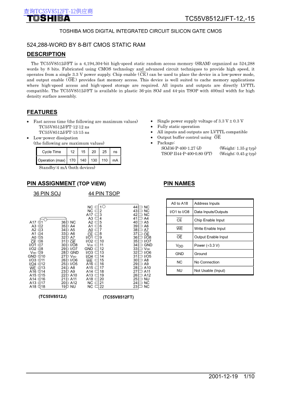
Page 1 Text Content
查询TC55V8512FT-12供应商
TC55V8512J/FT-12,-15
TOSHIBA MOS DIGITAL INTEGRATED CIRCUIT SILICON GATE CMOS
524,288-WORD BY 8-BIT CMOS STATIC RAM DESCRIPTION The TC55V8512J/FT is a 4,194,304-bit high-speed static random access memory (SRAM) organized as 524,288 words by 8 bits. Fabricated using CMOS technology and advanced circuit techniques to provide high speed, it
operates from a single 3.3 V power supply. Chip enable (CE ) can be used to place the device in a low-power mode,
and output enable ( OE ) provides fast memory access. This device is well suited to cache memory applications where high-speed access and high-speed storage are required. All inputs and outputs are directly LVTTL compatible. The TC55V8512J/FT is available in plastic 36-pin SOJ and 44-pin TSOP with 400mil width for high density surface assembly.
FEATURES
• Fast access time (the following are maximum values) • Single power supply voltage of 3.3 V ± 0.3 V TC55V8512J/FT-12:12 ns • Fully static operation TC55V8512J/FT-15:15 ns • All inputs and outputs are LVTTL compatible • Low-power dissipation • Output buffer control using OE (the following are maximum values) • Package: SOJ36-P-400-1.27 (J) (Weight: 1.35 g typ)
Cycle Time 12 15 20 25 ns
TSOP II44-P-400-0.80 (FT) (Weight: 0.45 g typ)
Operation (max) 170 140 130 110 m A Standby:4 m A (both devices)
PIN ASSIGNMENT (TOP VIEW) PIN NAMES 36 PIN SOJ 44 PIN TSOP
A0 to A18 Address Inputs
NC 1 44 NC NC 2 43 NC I/O1 to I/O8 Data Inputs/Outputs A17 3 42 NC A3 4 41 A4
CE Chip Enable Input
A17 1 36 NC A2 5 40 A5 A3 2 35 A4 A1 6 39 A6
WE Write Enable Input
A2 3 34 A5 A0 7 38 A7 A1 4 33 A6 8 37 OECE
A0 5 32 A7 I/O1 9 36 I/O8 OE Output Enable Input
CE 6 31 OE I/O2 10 35 I/O7 I/O1 7 30 I/O8 VDD 11 34 GND VDD Power (+3.3 V)
I/O2 8 29 I/O7 GND 12 33 VDD VDD 9 28 GND I/O3 13 32 I/O6
GND Ground
GND 10 27 VDD I/O4 14 31 I/O5 I/O3 11 26 I/O6 WE 15 30 A8
NC No Connection
WE 13 24 A8 A15 17 28 A10
A16 14 23 A9 A14 18 27 A11 NU Not Usable (Input)
A15 15 22 A10 A13 19 26 A12 A14 16 21 A11 A18 20 25 NU A13 17 20 A12 NC 21 24 NC A18 18 19 NU NC 22 23 NC
(TC55V8512J) (TC55V8512FT)
Page Summary Contents For Toshiba TOSHIBA TC55V8512J FT-12,-15 Data Sheet
Manual Details
| Brand | Toshiba |
|---|---|
| Pages | 10 |
| File Size | 151.86 KB |
| Published | June 02, 2026 |
Enter the captcha to get the download link:

Frequently Asked Questions
What is the recommended operating voltage range?
The recommended VDD Power Supply Voltage is 3.3V, with an acceptable range of 3.0V to 3.6V.
How can I put the device into a low-power mode?
You can use the Chip Enable (CE) input to place the device in a low-power mode (Standby).
What package types are available for this SRAM?
The TC55V8512J/FT is available in plastic 36-pin SOJ and 44-pin TSOP packages.
Is there a voltage restriction on the NU pin?
No, you must not apply a voltage higher than 0.8 V to the NU pin; it can be left unconnected or tied to GND.