# A B C D E F G H I J K L M N O P Q R S T U V W X Y Z

Texas Instruments TPS736xx Data Sheet Handbook

Summary

Featuring a unique NMOS topology, the TPS736xx is a versatile 400mA low-dropout regulator offering stable operation without external capacitors and ultra-low noise, ideal for portable battery-powered devices and noise-sensitive applications.
📄 Preview 📖 Table of Contents Contents PAGE OF 23

Page 1 Text Content

TPS736xx

www.ti.com

SBVS038K–SEPTEMBER 2003–REVISED SEPTEMBER

Cap-Free, NMOS, 400m A Low-Dropout Regulator

with Reverse Current Protection

FEATURES DESCRIPTION

Stable with No Output Capacitor or Any Value

The TPS736xx family of low-dropout (LDO) linear

or Type of Capacitor voltage regulators uses new topology: an NMOS

Input Voltage Range of 1.7V to 5.5V pass element in voltage-follower configuration. This•

topology is stable using output capacitors with low•

Ultra-Low Dropout Voltage: 75m V typ

ESR, and even allows operation without capacitor.

Excellent Load Transient Response—with or

It also provides high reverse blockage (low reverse

without Optional Output Capacitor current) and ground pin current that is nearly constant

over all values of output current.•

New NMOS Topology Delivers Low Reverse

Leakage Current

The TPS736xx uses an advanced Bi CMOS process

Low Noise: 30µVRMS typ (10Hz to 100k Hz) to yield high precision while delivering very low•

dropout voltages and low ground pin current. Current•

0.5% Initial Accuracy

consumption, when not enabled, is under 1µA and

1% Overall Accuracy Over Line, Load, and

ideal for portable applications. The extremely low

Temperature

output noise (30µVRMS with 0.1µF CNR) is ideal for

Less Than 1µA max IQ in Shutdown Mode powering VCOs. These devices are protected by•

thermal shutdown and foldback current limit.•

Thermal Shutdown and Specified Min/Max

Current Limit Protection

Available in Multiple Output Voltage Versions

Fixed Outputs of 1.20V to 4.3V

Adjustable Output from 1.20V to 5.5V

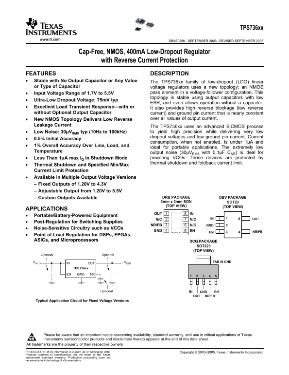
Custom Outputs Available DRB PACKAGE DBV PACKAGE

3mm 3mm SON SOT23 (TOP VIEW) (TOP VIEW)

APPLICATIONS

OUT IN

Portable/Battery-Powered Equipment

N/C N/C IN OUT1

Post-Regulation for Switching Supplies

NR/FB N/C GND

Noise-Sensitive Circuitry such as VCOs

GND EN

EN NR/FB

Point of Load Regulation for DSPs, FPGAs,

ASICs, and Microprocessors

DCQ PACKAGE SOT223 (TOP VIEW)

Optional Optional

VOUT TAB IS GND

IN OUTVIN TPS736xx GNDEN NR

Optional IN GND EN

OUT NR/FB

Typical Application Circuit for Fixed Voltage Versions

Please be aware that an important notice concerning availability, standard warranty, and use in critical applications of Texas

Instruments semiconductor products and disclaimers thereto appears at the end of this data sheet.

All trademarks are the property of their respective owners.

PRODUCTION DATA information is current as of publication date. Copyright 2003–2005, Texas Instruments Incorporated

Products conform to specifications per the terms of the Texas

Instruments standard warranty. Production processing does not

necessarily include testing of all parameters.

Page Summary Contents For Texas Instruments TPS736xx Data Sheet Handbook

Page 1 TPS736xx www.ti.com SBVS038K–SEPTEMBER 2003–REVISED SEPTEMBER Cap-Free, NMOS, 400m A Low-Dropout Regulator with Reverse Current Protection FEATURES DESCRIPTION Stable with No Output Capacitor or Any V...
Page 2 TPS736xx www.ti.com SBVS038K–SEPTEMBER 2003–REVISED SEPTEMBER This integrated circuit can be damaged by ESD. Texas Instruments recommends that all integrated circuits be handled with appropriate preca...
Page 3 TPS736xx www.ti.com SBVS038K–SEPTEMBER 2003–REVISED SEPTEMBER ELECTRICAL CHARACTERISTICS Over operating temperature range (TJ -40°C to +125°C), VIN VOUT(nom) 0.5V IOUT 10m A, VEN 1.7V, and COUT 0.1µF,...
Page 4 TPS736xx www.ti.com SBVS038K–SEPTEMBER 2003–REVISED SEPTEMBER FUNCTIONAL BLOCK DIAGRAMS 4MHz Charge Pump Thermal Protection Servo Bandgap Error Amp Current Limit OUT Figure 1. Fixed Voltage Version Ta...
Page 5 TPS736xx www.ti.com SBVS038K–SEPTEMBER 2003–REVISED SEPTEMBER PIN ASSIGNMENTS DBV PACKAGE DCQ PACKAGE DRB PACKAGE SOT223 3mm 3mm SON SOT23 (TOP VIEW) (TOP VIEW) (TOP VIEW) OUT IN TAB IS GND IN OUT1 NR...
Page 6 TPS736xx www.ti.com SBVS038K–SEPTEMBER 2003–REVISED SEPTEMBER ha ge in rc en to f U ni ts TYPICAL CHARACTERISTICS For all voltage versions, at TJ +25°C, VIN VOUT(nom) 0.5V, IOUT 10m A, VEN 1.7V, and C...
Page 7 TPS736xx www.ti.com SBVS038K–SEPTEMBER 2003–REVISED SEPTEMBER rr en Li it (m ur re t L im it (m (µ TYPICAL CHARACTERISTICS (continued) For all voltage versions, at TJ +25°C, VIN VOUT(nom) 0.5V, IOUT 1...
Page 8 TPS736xx www.ti.com SBVS038K–SEPTEMBER 2003–REVISED SEPTEMBER (R (µ /√ z) ip pl ej ec tio (d TYPICAL CHARACTERISTICS (continued) For all voltage versions, at TJ +25°C, VIN VOUT(nom) 0.5V, IOUT 10m A, ...
Page 9 TPS736xx www.ti.com SBVS038K–SEPTEMBER 2003–REVISED SEPTEMBER TYPICAL CHARACTERISTICS ol ts (continued) For all voltage versions, at TJ +25°C, VIN VOUT(nom) 0.5V, IOUT 10m A, VEN 1.7V, and COUT 0.1µF,...
Page 10 TPS736xx www.ti.com SBVS038K–SEPTEMBER 2003–REVISED SEPTEMBER TYPICAL CHARACTERISTICS (continued) For all voltage versions, at TJ +25°C, VIN VOUT(nom) 0.5V, IOUT 10m A, VEN 1.7V, and COUT 0.1µF, unles...
Page 11 TPS736xx www.ti.com SBVS038K–SEPTEMBER 2003–REVISED SEPTEMBER APPLICATION INFORMATION The TPS736xx belongs to family of new generation Input and Output Capacitor Requirements LDO regulators that use a...
Page 12 TPS736xx www.ti.com SBVS038K–SEPTEMBER 2003–REVISED SEPTEMBER This noise reduction effect is shown as RMS Noise For large step changes in load current, the TPS736xx Voltage vs CNR in the Typical Chara...
Page 13 TPS736xx www.ti.com SBVS038K–SEPTEMBER 2003–REVISED SEPTEMBER Reverse Current expected ambient temperature and worst-case load. The NMOS pass element of the TPS736xx provides The internal protection c...
Page 14 PACKAGE OPTION ADDENDUM www.ti.com 27-Feb-2006 PACKAGING INFORMATION Orderable Device Status Package Package Pins Package Eco Plan Lead/Ball Finish MSL Peak Temp Type Drawing Qty TPS73601DBVR ACTIVE S...
Page 15 PACKAGE OPTION ADDENDUM www.ti.com 27-Feb-2006 Orderable Device Status Package Package Pins Package Eco Plan Lead/Ball Finish MSL Peak Temp Type Drawing Qty TPS73615DRBRG4 ACTIVE SON DRB Green (Ro HS ...
Page 16 PACKAGE OPTION ADDENDUM www.ti.com 27-Feb-2006 Orderable Device Status Package Package Pins Package Eco Plan Lead/Ball Finish MSL Peak Temp Type Drawing Qty TPS73632DBVR ACTIVE SOT-23 DBV Green (Ro HS...
Page 17 PACKAGE OPTION ADDENDUM www.ti.com 27-Feb-2006 at high temperatures, TI Pb-Free products are suitable for use in specified lead-free processes. Pb-Free (Ro HS Exempt): This component has Ro HS exempti...
Page 23 IMPORTANT NOTICE Texas Instruments Incorporated and its subsidiaries (TI) reserve the right to make corrections, modifications, enhancements, improvements, and other changes to its products and servic...

Manual Details

Brand Texas Instruments
Pages 23
File Size 772.31 KB
Published June 15, 2026
3 views

Enter the captcha to get the download link:

captcha

Frequently Asked Questions

Does the TPS736xx require an output capacitor for stability?

No. It is stable with no output capacitor or any value or type of capacitor.

What is the input voltage range of the TPS736xx?

The input voltage range is 1.7V to 5.5V.

What is the overall accuracy of the TPS736xx over line, load, and temperature?

1% overall accuracy.

How much current does the TPS736xx consume in shutdown mode?

Less than 1µA maximum in shutdown mode.

Does the TPS736xx protect against reverse current?

Yes, it provides low reverse leakage current and high reverse blockage.